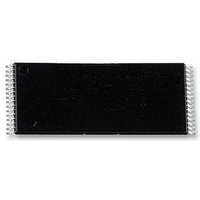
SST49LF008A-33-4C-WHE SILICON STORAGE TECHNOLOGY, SST49LF008A-33-4C-WHE Datasheet - Page 15

SST49LF008A-33-4C-WHE
Manufacturer Part Number
SST49LF008A-33-4C-WHE
Description
MEMORY, FLASH, 8M, SERIAL, 32TSOP
Manufacturer
SILICON STORAGE TECHNOLOGY
Datasheet
1.SST49LF008A-33-4C-WHE.pdf
(42 pages)
Specifications of SST49LF008A-33-4C-WHE
Memory Size
8Mbit
Clock Frequency
33MHz
Supply Voltage Range
3V To 3.6V
Memory Case Style
TSOP
No. Of Pins
32
Operating Temperature Range
0°C To +70°C
Svhc
No SVHC (18-Jun-2010)
Memory Type
Flash
Memory Configuration
1024K X 8
Interface Type
Parallel
Rohs Compliant
Yes
Lead Free Status / RoHS Status
Lead free / RoHS Compliant
Available stocks
Company
Part Number
Manufacturer
Quantity
Price
Part Number:
SST49LF008A-33-4C-WHE
Manufacturer:
SST
Quantity:
20 000
Part Number:
SST49LF008A-33-4C-WHE-T
Manufacturer:
SST
Quantity:
20 000
8 Mbit Firmware Hub
SST49LF008A
Data# Polling (DQ
When the SST49LF008A device is in the internal Program
operation, any attempt to read DQ
plement of the true data. Once the Program operation is
completed, DQ
though DQ
completion of an internal Write operation, the remaining
data outputs may still be invalid: valid data on the entire
data bus will appear in subsequent successive Read
cycles after an interval of 1 µs. During internal Erase opera-
tion, any attempt to read DQ
internal Erase operation is completed, DQ
‘1’. Proper status will not be given using Data# Polling if the
address is in the invalid range.
Toggle Bit (DQ
During the internal Program or Erase operation, any con-
secutive attempts to read DQ
‘0’s and ‘1’s, i.e., toggling between 0 and 1. When the
internal Program or Erase operation is completed, the
toggling will stop.
Multiple Device Selection
The four ID pins, ID[3:0], allow multiple devices to be
attached to the same bus by using different ID strapping in
a system. When the SST49LF008A is used as a boot
device, ID[3:0] must be strapped as 0000, all subsequent
devices should use a sequential up-count strapping (i.e.
0001, 0010, 0011, etc.). The SST49LF008A will compare
the strapping values, if there is a mismatch, the device will
ignore the remainder of the cycle and go into standby
mode. For further information regarding FWH device map-
ping and paging, please refer to the Intel 82801(ICH) I/O
Controller Hub documentation. Since there is no ID support
in PP Mode, to program multiple devices a stand-alone
PROM programmer is recommended.
REGISTERS
There are three types of registers available on the
SST49LF008A, the General Purpose Inputs register, Block
Locking registers and the JEDEC ID registers. These regis-
ters appear at their respective address location in the 4
GByte system memory map. Unused register locations will
read as 00H. Attempts to read or write to any registers dur-
ing internal Write operations will be ignored.
©2006 Silicon Storage Technology, Inc.
7
may have valid data immediately following the
7
will produce true data. Note that even
6
)
7
)
7
will produce a ‘0’. Once the
6
will produce alternating
7
will produce the com-
7
will produce a
15
General Purpose Inputs Register
The GPI_REG (General Purpose Inputs Register) passes
the state of FGPI[4:0] pins at power-up on the
SST49LF008A. It is recommended that the FGPI[4:0] pins
are in the desired state before FWH4 is brought low for the
beginning of the bus cycle, and remain in that state until the
end of the cycle. There is no default value since this is a
pass-through register. The GPI register for the boot device
appears at FFBC0100H in the 4 GByte system memory
map, and will appear elsewhere if the device is not the boot
device. Register is not available for read when the device is
in Erase/Program operation. See Table 5 for the GPI_REG
bits and function.
TABLE 5: General Purpose Inputs Register
Block Locking Registers
SST49LF008A provides software controlled lock pro-
tection through a set of Block Locking registers. The
Block Locking Registers are read/write registers and it
is accessible through standard addressable memory
locations specified in Table 6. Unused register loca-
tions will read as 00H.
7:5
Bit
4
3
2
1
0
Function
Reserved
FGPI[4]
Reads status of general
purpose input pin
FGPI[3]
Reads status of general
purpose input pin
FGPI[2]
Reads status of general
purpose input pin
FGPI[1]
Reads status of general
purpose input pin
FGPI[0]
Reads status of general
purpose input pin
32-PLCC
30
3
4
5
6
-
32-TSOP
S71161-11-000
Pin #
11
12
13
14
6
-
Data Sheet
40-TSOP
T5.3 1161
15
16
17
18
7
-
3/06


