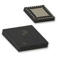
LPC1113FHN33/301 NXP Semiconductors, LPC1113FHN33/301 Datasheet - Page 19

LPC1113FHN33/301
Manufacturer Part Number
LPC1113FHN33/301
Description
MCU, 32BIT, 24KFLASH, CORTEX-M0, 33HVQFN
Manufacturer
NXP Semiconductors
Datasheet
1.LPC1111FHN33101.pdf
(66 pages)
Specifications of LPC1113FHN33/301
Controller Family/series
ARM Cortex-M0
No. Of I/o's
28
Ram Memory Size
8KB
Cpu Speed
50MHz
No. Of Timers
4
Core Size
32bit
Program Memory Size
24KB
Oscillator Type
External, Internal
Lead Free Status / RoHS Status
Lead free / RoHS Compliant
Available stocks
Company
Part Number
Manufacturer
Quantity
Price
Company:
Part Number:
LPC1113FHN33/301
Manufacturer:
NXP
Quantity:
5 000
Company:
Part Number:
LPC1113FHN33/301
Manufacturer:
NXP
Quantity:
2 000
Part Number:
LPC1113FHN33/301
Manufacturer:
NXP/恩智浦
Quantity:
20 000
NXP Semiconductors
Table 5.
[1]
[2]
[3]
[4]
[5]
[6]
LPC1111_12_13_14
Product data sheet
Symbol
PIO3_5
V
XTALIN
XTALOUT
V
DD
SS
Pin state at reset for default function: I = Input; O = Output; PU = internal pull-up enabled; IA = inactive, no pull-up/down enabled.
See
reset the chip and wake up from Deep power-down mode. An external pull-up resistor is required on this pin for the Deep power-down
mode.
5 V tolerant pad providing digital I/O functions with configurable pull-up/pull-down resistors and configurable hysteresis (see
I
5 V tolerant pad providing digital I/O functions with configurable pull-up/pull-down resistors, configurable hysteresis, and analog input.
When configured as a ADC input, digital section of the pad is disabled, and the pin is not 5 V tolerant (see
When the system oscillator is not used, connect XTALIN and XTALOUT as follows: XTALIN can be left floating or can be grounded
(grounding is preferred to reduce susceptibility to noise). XTALOUT should be left floating.
2
C-bus pads compliant with the I
Figure 33
LPC1111/12/13/14 pin description table (HVQFN33 package)
for the reset pad configuration. RESET functionality is not available in Deep power-down mode. Use the WAKEUP pin to
Pin
14
6; 29 -
4
5
33
[6]
[6]
[3]
Start
logic
input
no
-
-
-
2
C-bus specification for I
Type Reset
I/O
I
I
O
-
All information provided in this document is subject to legal disclaimers.
state
[1]
I;PU
-
-
-
-
Rev. 4 — 10 February 2011
Description
PIO3_5 — General purpose digital input/output pin.
3.3 V supply voltage to the internal regulator, the external rail, and the
ADC. Also used as the ADC reference voltage.
Input to the oscillator circuit and internal clock generator circuits. Input
voltage must not exceed 1.8 V.
Output from the oscillator amplifier.
Thermal pad. Connect to ground.
2
C standard mode and I
…continued
2
C Fast-mode Plus.
32-bit ARM Cortex-M0 microcontroller
LPC1111/12/13/14
Figure
© NXP B.V. 2011. All rights reserved.
32).
Figure
19 of 66
32).


