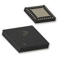
LPC1113FHN33/301 NXP Semiconductors, LPC1113FHN33/301 Datasheet - Page 52

LPC1113FHN33/301
Manufacturer Part Number
LPC1113FHN33/301
Description
MCU, 32BIT, 24KFLASH, CORTEX-M0, 33HVQFN
Manufacturer
NXP Semiconductors
Datasheet
1.LPC1111FHN33101.pdf
(66 pages)
Specifications of LPC1113FHN33/301
Controller Family/series
ARM Cortex-M0
No. Of I/o's
28
Ram Memory Size
8KB
Cpu Speed
50MHz
No. Of Timers
4
Core Size
32bit
Program Memory Size
24KB
Oscillator Type
External, Internal
Lead Free Status / RoHS Status
Lead free / RoHS Compliant
Available stocks
Company
Part Number
Manufacturer
Quantity
Price
Company:
Part Number:
LPC1113FHN33/301
Manufacturer:
NXP
Quantity:
5 000
Company:
Part Number:
LPC1113FHN33/301
Manufacturer:
NXP
Quantity:
2 000
Part Number:
LPC1113FHN33/301
Manufacturer:
NXP/恩智浦
Quantity:
20 000
NXP Semiconductors
Table 18.
LPC1111_12_13_14
Product data sheet
Symbol
SPI master (in SPI mode)
T
t
t
t
t
SPI slave (in SPI mode)
DS
DH
v(Q)
h(Q)
Fig 27. I
cy(clk)
SDA
SCL
2
C-bus pins clock timing
Dynamic characteristics of SPI pins in SPI mode
Parameter
clock cycle time
data set-up time
data hold time
data output valid time in SPI mode
data output hold time in SPI mode
70 %
30 %
S
10.7 SPI interfaces
t
f
t
f
70 %
[6]
[7]
[8]
[9]
[10] A Fast-mode I
30 %
The maximum t
output stage t
SDA and the SCL pins and the SDA/SCL bus lines without exceeding the maximum specified t
In Fast-mode Plus, fall time is specified the same for both output stage and bus timing. If series resistors
are used, designers should allow for this when considering bus timing.
The maximum t
the maximum of t
the device does not stretch the LOW period (t
data must be valid by the set-up time before it releases the clock.
t
transmission and the acknowledge.
t
LOW period of the SCL signal. If such a device does stretch the LOW period of the SCL signal, it must
output the next data bit to the SDA line t
Standard-mode I
meet this set-up time.
1 / f
SU;DAT
SU;DAT
SCL
Conditions
when only receiving
when only transmitting
in SPI mode
in SPI mode
is the data set-up time that is measured with respect to the rising edge of SCL; applies to data in
= 250 ns must then be met. This will automatically be the case if the device does not stretch the
t
2.4 V ≤ V
2.0 V ≤ V
1.8 V ≤ V
HD;DAT
70 %
30 %
70 %
f
30 %
2
All information provided in this document is subject to legal disclaimers.
is specified at 250 ns. This allows series protection resistors to be connected in between the
C-bus device can be used in a Standard-mode I
HD;DAT
f
for the SDA and SCL bus lines is specified at 300 ns. The maximum fall time for the SDA
2
VD;DAT
C-bus specification) before the SCL line is released. Also the acknowledge timing must
t
SU;DAT
DD
DD
DD
could be 3.45 μs and 0.9 μs for Standard-mode and Fast-mode but must be less than
≤ 3.6 V
< 2.4 V
< 2.0 V
Rev. 4 — 10 February 2011
or t
VD;ACK
70 %
30 %
[1]
[1]
[2]
[2]
[2]
[2]
[2]
[2]
by a transition time (see UM10204). This maximum must only be met if
t
LOW
r(max)
Min
40
27.8
15
20
24
0
-
0
+ t
LOW
SU;DAT
) of the SCL signal. If the clock stretches the SCL, the
t
HIGH
= 1000 + 250 = 1250 ns (according to the
32-bit ARM Cortex-M0 microcontroller
70 %
30 %
LPC1111/12/13/14
t
VD;DAT
2
Typ
-
-
-
-
-
-
C-bus system but the requirement
Max
-
-
-
-
10
-
© NXP B.V. 2011. All rights reserved.
002aaf425
f
.
52 of 66
ns
Unit
ns
ns
ns
ns
ns
ns
ns


