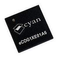
ECOG1XE01A6 CYAN, ECOG1XE01A6 Datasheet - Page 18

ECOG1XE01A6
Manufacturer Part Number
ECOG1XE01A6
Description
IC, 16BIT MCU, ECOG1X, 70MHZ, QFN-68
Manufacturer
CYAN
Datasheet
1.ECOG1X14Z5.pdf
(95 pages)
Specifications of ECOG1XE01A6
Controller Family/series
ECOG1X
No. Of I/o's
20
Ram Memory Size
8KB
Cpu Speed
70MHz
No. Of Timers
8
Digital Ic Case Style
QFN
Core Size
16 Bit
Program Memory Size
64KB
Embedded Interface Type
I2C, JTAG, SPI, UART
Rohs Compliant
Yes
Lead Free Status / RoHS Status
Lead free / RoHS Compliant
Version 1.15
1
2
3
4
5
6
7
8
9
10
11
18
Label
Rext
ULPI_CLK
ULPI_DATA0-7
USB_n
USB_p
USBVDD
ULPI_STOP
ULPI_NXT
ULPI_DIR
ULPI_RST
VDD
VPP
Vref
11
The eICE_LOADB pin has an internal pull-up resistor connected to VDD with a value of 20k Ω -100k Ω . This is
sufficient for normal operation when the eICE debug port is not in use or disconnected. When the eICE port is used
for debugging, a 4.7k Ω pull-up resistor is recommended to reduce the rise time on this open-drain signal and
increase the speed of eICE data transfers. If the system is used with an external eICE programming adaptor, then
the external adaptor has the 4.7k Ω pull-up resistor fitted, and the target system does not need any additional pull-up
resistor connected to this signal.
It is also recommended that the eICE input signals (eICE_CLK, eICE_MOSI) are connected to GND via 100k Ω pull-
down resistors as a precaution against noise when the eICE port is not in use or disconnected.
The FIL pin requires external low pass filter components for the low frequency PLL to be fitted. The filter consists of
a 2.2nF capacitor from FIL to GND, in parallel with a 68nF capacitor and an 8.2k Ω resistor in series.
The external quartz crystal used with the 8MHz high reference oscillator requires two load capacitors. The
maximum load capacitance value for the high reference oscillator is 32pF, including any package and stray
capacitance due to the circuit board layout. The recommended load capacitor value is 22pF. If an external clock
source is used instead of the 8MHz quartz crystal oscillator, then High_XTAL_Out is not connected and the external
clock signal is connected to High_XTAL_In. If the high reference clock is not required, then High_XTAL_Out is not
connected and High_XTAL_In is connected to AGND via a 10k Ω resistor.
The external quartz crystal used with the 32.768kHz low reference oscillator requires two load capacitors. The
maximum load capacitance value for the low reference oscillator is 25pF, including any package and stray
capacitance due to the circuit board layout. The recommended load capacitor value is 10pF. If an external clock
source is used instead of the 32.768kHz quartz crystal oscillator, then Low_XTAL_Out is not connected and the
external clock signal is connected to Low_XTAL_In. If the low reference clock is not required, then Low_XTAL_Out
is not connected and Low_XTAL_In is connected to AGND via a 10k Ω resistor.
On smaller package variants (68QFN, 100QFN), the nReset pin is bidirectional. It is driven low internally as an
open-drain output by the on-chip power-on reset supply voltage sense circuit, and is also connected as an input to
the device from the pin. This allows the use of an external reset circuit if required. The nReset input has a Schmitt
trigger input circuit and an internal pull-up resistor.
On larger package variants (208BGA), the nReset_Out and nReset_In pins are not connected internally. This
allows the use of an external reset circuit. An active low power-on reset signal must be connected to nReset_In for
correct operation of the device, from the internal reset circuit or an external power-on reset circuit. To use the
internal power-on reset circuit, connect nReset_Out to nReset_In, either directly or via external logic for any
additional external reset source such as a pushbutton switch. The nReset_In input has a Schmitt trigger input circuit
and an internal pull-up resistor. The nReset_Out output is open-drain with an internal pull-up resistor, and can be
used in a wired-OR connection with an external power-on reset if the external device also has an active-low open-
drain output.
The nTest pin is not used in normal applications and should be connected to VDD, directly or via a pull-up resistor.
The Rext pin for the external resistor to set the frequency of the relaxation oscillator is available only on the
208BGA package. For all devices in the smaller 68QFN and 100QFN packages, the relaxation oscillator runs at the
frequency corresponding to an open circuit at Rext with the external resistor not fitted.
The ULPI_CLK input should be pulled low or tied to GND if the ULPI high-speed USB connection is not used.
The VPP pin is used with a higher voltage supply to support faster programming of the internal flash memory via
JTAG. If this function is not required, then the VPP pin should be connected to GND to minimise power
consumption in normal operation. If this function is required, then connect VPP to GND via a pull-down resistor or
jumper link so that the fast programming supply can be connected.
Applications which use the analogue inputs or outputs with the internal reference voltage must have external
decoupling capacitors connected to the Vref pin. The recommended decoupling on this pin is a 100nF ceramic
capacitor in parallel with a 4.7µF tantalum or aluminium electrolytic capacitor.
8
10
9
Function
External resistor to set relaxation oscillator frequency
USB ULPI Clock input
USB ULPI Data bus
USB data negative
USB data positive
USB power supply 3.3V
USB ULPI Stop
USB ULPI Next
USB ULPI Direction
USB ULPI Reset
Digital power supply 3.3V
Flash memory high speed programming power supply
Analogue reference voltage
eCOG and CyanIDE are registered trademarks of Cyan Holdings plc
eCOG1X Microcontroller Product Family
www.cyantechnology.com
Table 12: Pin functions
4 August 2009
PWR
PWR
PWR
I/O
I/O
I/O
I/O
O
I
I
I


