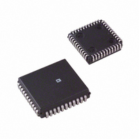
AD2S82ALPZ Analog Devices Inc, AD2S82ALPZ Datasheet - Page 10

AD2S82ALPZ
Manufacturer Part Number
AD2S82ALPZ
Description
2 ARC MIN PLCC MONO R/D
Manufacturer
Analog Devices Inc
Type
R/D Converterr
Datasheet
1.AD2S80AJD.pdf
(16 pages)
Specifications of AD2S82ALPZ
Rohs Compliant
YES
Input Type
Parallel
Output Type
Digital
Interface
Parallel
Current - Supply
30mA
Mounting Type
Surface Mount
Package / Case
44-PLCC
Lead Free Status / RoHS Status
Lead free / RoHS Compliant
Available stocks
Company
Part Number
Manufacturer
Quantity
Price
Company:
Part Number:
AD2S82ALPZ
Manufacturer:
MAXIM
Quantity:
9 739
Company:
Part Number:
AD2S82ALPZ
Manufacturer:
Analog Devices Inc
Quantity:
10 000
Part Number:
AD2S82ALPZ
Manufacturer:
ADI/亚德诺
Quantity:
20 000
AD2S80A
CIRCUIT FUNCTIONS AND DYNAMIC PERFORMANCE
The AD2S80A allows the user greater flexibility in choosing the
dynamic characteristics of the resolver-to-digital conversion to
ensure the optimum system performance. The characteristics
are set by the external components shown in Figure 1, and the
section “COMPONENT SELECTION” explains how to select
desired maximum tracking rate and bandwidth values. The
following paragraphs explain in greater detail the circuit of the
AD2S80A and the variations in the dynamic performance avail-
able to the user.
Loop Compensation
The AD2S80A (connected as shown in Figure 1) operates as a
Type 2 tracking servo loop where the VCO/counter combination
and Integrator perform the two integration functions inherent in
a Type 2 loop.
Ratio Multiplier
The ratio multiplier is the input section of the AD2S80A and
compares the signal from the resolver input angle, θ, to the
digital angle, φ, held in the counter. Any difference between
these two angles results in an analog voltage at the AC ERROR
OUTPUT. This circuit function has historically been called
a “Control Transformer” as it was originally performed by an
electromechanical device known by that name.
The AC ERROR signal is given by
where ω = 2 π f
A1, the gain of the ratio multiplier stage is 14.5.
So for 2 V rms inputs signals
AC ERROR output in volts/(bit of error)
where n = bits per rev
giving an AC ERROR output
f
REF
= reference frequency
= 1,024 for 10 bits resolution
= 4,096 for 12 bits
= 16,384 for 14 bits
= 65,536 for 16 bits
= 178 mV/bit @ 10 bits resolution
= 44.5 mV/bit @ 12 bits
= 11.125 mV/bit @ 14 bits
= 2.78 mV/bit @ 16 bits
REF
= 2 × sin
A1 sin (θ–φ) sin ω t
cos
sin
360
sin
sin
n
× A1
t
t
DIGITAL
MULTIPLIER
RATIO
A
1
sin ( –
DIRECTION
CLOCK
AC ERROR
) sin
Additional compensation in the form of a pole/zero pair is
required to stabilize any Type 2 loop to avoid the loop gain
characteristic crossing the 0 dB axis with 180° of additional
phase lag, as shown in Figure 5.
This compensation is implemented by the integrator compo-
nents (R4, C4, R5, C5).
The overall response of such a system is that of a unity gain
second order low pass filter, with the angle of the resolver as the
input and the digital position data as the output.
The AD2S80A does not have to be connected as tracking con-
verter, parts of the circuit can be used independently. This is
particularly true of the Ratio Multiplier which can be used as a
control transformer (see Application Note).
A block diagram of the AD2S80A is given in Figure 3.
The ratio multiplier will work in exactly the same way whether
the AD2S80A is connected as a tracking converter or as a con-
trol transformer, where data is preset into the counters using the
DATA LOAD pin.
HF Filter
The AC ERROR OUTPUT may be fed to the PSD via a simple
ac coupling network (R2, C1) to remove any dc offset at this
point. Note, however, that the PSD of the AD2S80A is a wide-
band demodulator and is capable of aliasing HF noise down to
within the loop bandwidth. This is most likely to happen where
the resolver is situated in particularly noisy environments, and
the user is advised to fit a simple HF filter R1, C2 prior to the
phase sensitive demodulator.
The attenuation and frequency response of a filter will affect the
loop gain and must be taken into account in deriving the loop
transfer function. The suggested filter (R1, C1, R2, C2) is
shown in Figure 1 and gives an attenuation at the reference
frequency (f
demodulator .
Values of components used in the filter must be chosen to ensure
that the phase shift at f
reference phase shift of the converter.
Phase Sensitive Demodulator
The phase sensitive demodulator is effectively ideal and devel-
ops a mean dc output at the DEMODULATOR OUTPUT
pin of
t
DEMODULATOR
SENSITIVE
±2 2
PHASE
VCO
π
REF
× (DEMODULATOR INPUT rms voltage )
) of 3 times at the input to the phase sensitive
R4
R6
INTEGRATOR
REF
R5
C4
is within the allowable signal to
C5
VELOCITY


