AD2S82ALPZ Analog Devices Inc, AD2S82ALPZ Datasheet - Page 9
AD2S82ALPZ
Manufacturer Part Number
AD2S82ALPZ
Description
2 ARC MIN PLCC MONO R/D
Manufacturer
Analog Devices Inc
Type
R/D Converterr
Datasheet
1.AD2S80AJD.pdf
(16 pages)
Specifications of AD2S82ALPZ
Rohs Compliant
YES
Input Type
Parallel
Output Type
Digital
Interface
Parallel
Current - Supply
30mA
Mounting Type
Surface Mount
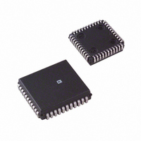
Package / Case
44-PLCC
Lead Free Status / RoHS Status
Lead free / RoHS Compliant
Available stocks
Company
Part Number
Manufacturer
Quantity
Price
Company:

Part Number:
AD2S82ALPZ
Manufacturer:
MAXIM
Quantity:
9 739
Company:
Part Number:
AD2S82ALPZ
Manufacturer:
Analog Devices Inc
Quantity:
10 000
Part Number:
AD2S82ALPZ
Manufacturer:
ADI/亚德诺
Quantity:
20 000


DATA TRANSFER
To transfer data the INHIBIT input should be used. The data
will be valid 600 ns after the application of a logic “LO” to the
INHIBIT. This is regardless of the time when the INHIBIT is
applied and allows time for an active BUSY to clear. By using
the ENABLE input the two bytes of data can be transferred
after which the INHIBIT should be returned to a logic “HI”
state to enable the output latches to be updated.
BUSY Output
The validity of the output data is indicated by the state of the
BUSY output. When the input to the converter is changing, the
signal appearing on the BUSY output is a series of pulses at
TTL level. A BUSY pulse is initiated each time the input moves
by the analog equivalent of one LSB and the internal counter is
incremented or decremented.
INHIBIT Input
The INHIBIT logic input only inhibits the data transfer from
the up-down counter to the output latches and, therefore, does
not interrupt the operation of the tracking loop. Releasing the
INHIBIT automatically generates a BUSY pulse to refresh the
output data.
ENABLE Input
The ENABLE input determines the state of the output data. A
logic “HI” maintains the output data pins in the high imped-
ance condition, and the application of a logic “LO” presents the
data in the latches to the output pins. The operation of the
ENABLE has no effect on the conversion process.
BYTE SELECT Input
The BYTE SELECT input selects the byte of the position data
to be presented at the data output DB1 to DB8. The least signifi-
cant byte will be presented on data output DB9 to DB16 (with
the ENABLE input taken to a logic “LO”) regardless of the
state of the BYTE SELECT pin. Note that when the AD2S80A is
used with a resolution less than 16 bits the unused data lines are
pulled to a logic “LO.” A logic “HI” on the BYTE SELECT input
will present the eight most significant data bits on data output
DB1 and DB8. A logic “LO” will present the least significant
byte on data outputs 1 to 8, i.e., data outputs 1 to 8 will dupli-
cate data outputs 9 to 16.
The operation of the BYTE SELECT has no effect on the con-
version process of the converter.
RIPPLE CLOCK
As the output of the converter passes through the major carry,
i.e., all “1s” to all “0s” or the converse, a positive going edge on
the RIPPLE CLOCK (RC) output is initiated indicating that a
revolution, or a pitch, of the input has been completed.
The minimum pulse width of the ripple clock is 300 ns. RIPPLE
CLOCK is normally set high before a BUSY pulse and resets
before the next positive going edge of the next consecutive pulse.
The only exception to this is when DIR changes while the
RIPPLE CLOCK is high. Resetting of the RIPPLE clock will
only occur if the DIR remains stable for two consecutive posi-
tive BUSY pulse edges.
If the AD2S80A is being used in a pitch and revolution count-
ing application, the ripple and busy will need to be gated to
prevent false decrement or increment (see Figure 2).
RIPPLE CLOCK is unaffected by INHIBIT.
DIRECTION Output
The DIRECTION (DIR) logic output indicates the direction of
the input rotation. Any change in the state of DIR precedes the
corresponding BUSY, DATA and RIPPLE CLOCK updates.
DIR can be considered as an asynchronous output and can
make multiple changes in state between two consecutive LSB
update cycles. This corresponds to a change in input rotation
direction but less than 1 LSB.
RIPPLE
CLOCK
BUSY
ENABLE
SELECT
NOTE: DO NOT USE ABOVE CCT WHEN INHIBIT IS "LO."
RIPPLE
CLOCK
INHIBIT
INHIBIT
BUSY
DATA
DATA
BYTE
DATA
DIR
5k
V
V
H
H
5V
V
Z
V
DIGITAL TIMING
t
V
t
t
H
7
IN4148
IN4148
L
t
6
8
2
V
L
V
V
L
5V
t
H
t
12
t
V
t
4
t
5
10
L
11
t
1
t
10k
V
9
INHIBIT
INHIBIT
ENABLE
ENABLE
H
V
L
2N3904
V
V
1k
0V
H
L
V
H
t
13
V
AD2S80A
t
L
3
TO COUNTER
(CLOCK)
V
V
H
L
Related parts for AD2S82ALPZ
Image
Part Number
Description
Manufacturer
Datasheet
Request
R

Part Number:
Description:
±1.7g Dual-Axis IMEMS Accelerometer Evaluation Board
Manufacturer:
Analog Devices Inc
Datasheet:

Part Number:
Description:
Inertial Sensor Evaluation System
Manufacturer:
Analog Devices Inc
Datasheet:
Part Number:
Description:
Manufacturer:
Analog Devices Inc
Datasheet:
Part Number:
Description:
Manufacturer:
Analog Devices Inc
Datasheet:
Part Number:
Description:
Manufacturer:
Analog Devices Inc
Datasheet:
Part Number:
Description:
Manufacturer:
Analog Devices Inc
Datasheet:
Part Number:
Description:
Manufacturer:
Analog Devices Inc
Datasheet:
Part Number:
Description:
Manufacturer:
Analog Devices Inc
Datasheet:
Part Number:
Description:
Manufacturer:
Analog Devices Inc
Datasheet:
Part Number:
Description:
Manufacturer:
Analog Devices Inc
Datasheet:
Part Number:
Description:
Manufacturer:
Analog Devices Inc
Datasheet:
Part Number:
Description:
Manufacturer:
Analog Devices Inc
Datasheet:
Part Number:
Description:
Manufacturer:
Analog Devices Inc
Datasheet: