AD2S82ALPZ Analog Devices Inc, AD2S82ALPZ Datasheet - Page 6
AD2S82ALPZ
Manufacturer Part Number
AD2S82ALPZ
Description
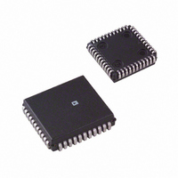
2 ARC MIN PLCC MONO R/D
Manufacturer
Analog Devices Inc
Type
R/D Converterr
Datasheet
1.AD2S80AJD.pdf
(16 pages)
Specifications of AD2S82ALPZ
Rohs Compliant
YES
Input Type
Parallel
Output Type
Digital
Interface
Parallel
Current - Supply
30mA
Mounting Type
Surface Mount
Package / Case
44-PLCC
Lead Free Status / RoHS Status
Lead free / RoHS Compliant
Available stocks
Company
Part Number
Manufacturer
Quantity
Price
Company:

Part Number:
AD2S82ALPZ
Manufacturer:
MAXIM
Quantity:
9 739
Company:
Part Number:
AD2S82ALPZ
Manufacturer:
Analog Devices Inc
Quantity:
10 000
Part Number:
AD2S82ALPZ
Manufacturer:
ADI/亚德诺
Quantity:
20 000


AD2S80A
CONNECTING THE CONVERTER
The power supply voltages connected to +V
should be +12 V dc and –12 V dc and must not be reversed.
The voltage applied to V
It is recommended that the decoupling capacitors are connected
in parallel between the power lines +V
GROUND adjacent to the converter. Recommended values
are 100 nF (ceramic) and 10 µF (tantalum). Also capacitors of
100 nF and 10 µF should be connected between +V
DIGITAL GROUND adjacent to the converter.
When more than one converter is used on a card, then separate
decoupling capacitors should be used for each converter.
The resolver connections should be made to the SIN and COS
inputs, REFERENCE INPUT and SIGNAL GROUND as
shown in Figure 7 and described in section “CONNECTING
THE RESOLVER.”
The two signal ground wires from the resolver should be joined
at the SIGNAL GROUND pin of the converter to minimize the
coupling between the sine and cosine signals. For this reason it
is also recommended that the resolver is connected using indi-
vidually screened twisted pair cables with the sine, cosine and
reference signals twisted separately.
SIG GND
RIPPLE
+12V
–12V
COS
GND
CLK
SIN
DATA
LOAD
A2
A1
SC1 SC2
L
can be 5 V dc to +V
SWITCHING
SEGMENT
ENABLE
16-BIT UP/DOWN COUNTER
OUTPUT DATA LATCH
S
, –V
R-2R DAC
16 DATA BITS
S
S
and –V
S
and ANALOG
.
AC ERROR O/P
S
L
pins
A3
and
C1
R1
HF FILTER
AD2S80A
SELECT
DEMOD
BYTE
R2
C2
I/P
5V
REFERENCE
SIGNAL GROUND and ANALOG GROUND are connected
internally. ANALOG GROUND and DIGITAL GROUND
must be connected externally.
The external components required should be connected as
shown in Figure 1.
CONVERTER RESOLUTION
Two major areas of the AD2S80A specification can be selected
by the user to optimize the total system performance. The reso-
lution of the digital output is set by the logic state of the inputs
SC1 and SC2 to be 10, 12, 14, or 16 bits; and the dynamic
characteristics of bandwidth and tracking rate are selected by the
choice of external components.
The choice of the resolution will affect the values of R4 and R6
which scale the inputs to the integrator and the VCO respectively
(see section COMPONENT SELECTION). If the resolution is
changed, then new values of R4 and R6 must be switched into
the circuit.
Note: When changing resolution under dynamic conditions, do
it when the BUSY is low, i.e., when Data is not changing.
DETECTOR
SENSITIVE
PHASE
GND
I/P
DIG
R3
C3
BUSY
TRANSFER LOGIC
DEMOD
O/P
VCO + DATA
DIRN INHIBIT
R4
+12V
INTEGRATOR
OFFSET ADJUST
INTEGRATOR
I/P
R9
O/P
R8
VCO
I/P
–12V
R6
BANDWIDTH
SELECTION
R7
C4
C6
TRACKING
RATE
SELECTION
C5
R5
VELOCITY
SIGNAL
Related parts for AD2S82ALPZ
Image
Part Number
Description
Manufacturer
Datasheet
Request
R

Part Number:
Description:
±1.7g Dual-Axis IMEMS Accelerometer Evaluation Board
Manufacturer:
Analog Devices Inc
Datasheet:

Part Number:
Description:
Inertial Sensor Evaluation System
Manufacturer:
Analog Devices Inc
Datasheet:
Part Number:
Description:
Manufacturer:
Analog Devices Inc
Datasheet:
Part Number:
Description:
Manufacturer:
Analog Devices Inc
Datasheet:
Part Number:
Description:
Manufacturer:
Analog Devices Inc
Datasheet:
Part Number:
Description:
Manufacturer:
Analog Devices Inc
Datasheet:
Part Number:
Description:
Manufacturer:
Analog Devices Inc
Datasheet:
Part Number:
Description:
Manufacturer:
Analog Devices Inc
Datasheet:
Part Number:
Description:
Manufacturer:
Analog Devices Inc
Datasheet:
Part Number:
Description:
Manufacturer:
Analog Devices Inc
Datasheet:
Part Number:
Description:
Manufacturer:
Analog Devices Inc
Datasheet:
Part Number:
Description:
Manufacturer:
Analog Devices Inc
Datasheet:
Part Number:
Description:
Manufacturer:
Analog Devices Inc
Datasheet: