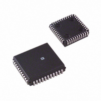
AD2S82ALPZ Analog Devices Inc, AD2S82ALPZ Datasheet - Page 11

AD2S82ALPZ
Manufacturer Part Number
AD2S82ALPZ
Description
2 ARC MIN PLCC MONO R/D
Manufacturer
Analog Devices Inc
Type
R/D Converterr
Datasheet
1.AD2S80AJD.pdf
(16 pages)
Specifications of AD2S82ALPZ
Rohs Compliant
YES
Input Type
Parallel
Output Type
Digital
Interface
Parallel
Current - Supply
30mA
Mounting Type
Surface Mount
Package / Case
44-PLCC
Lead Free Status / RoHS Status
Lead free / RoHS Compliant
Available stocks
Company
Part Number
Manufacturer
Quantity
Price
Company:
Part Number:
AD2S82ALPZ
Manufacturer:
MAXIM
Quantity:
9 739
Company:
Part Number:
AD2S82ALPZ
Manufacturer:
Analog Devices Inc
Quantity:
10 000
Part Number:
AD2S82ALPZ
Manufacturer:
ADI/亚德诺
Quantity:
20 000
for sinusoidal signals in phase or antiphase with the reference
(for a square wave the DEMODULATOR OUTPUT voltage
will equal the DEMODULATOR INPUT). This provides a
signal at the DEMODULATOR OUTPUT which is a dc level
proportional to the positional error of the converter.
DC Error Scaling = 160 mV/bit (10 bits resolution)
When the tracking loop is closed, this error is nulled to zero
unless the converter input angle is accelerating.
Integrator
The integrator components (R4, C4, R5, C5) are external to the
AD2S80A to allow the user to determine the optimum dynamic
characteristics for any given application. The section “COMPO-
NENT SELECTION” explains how to select components for a
chosen bandwidth.
Since the output from the integrator is fed to the VCO INPUT,
it is proportional to velocity (rate of change of output angle) and
can be scaled by selection of R6, the VCO input resistor. This is
explained in the section “VOLTAGE CONTROLLED OSCIL-
LATOR (VCO)” below.
To prevent the converter from “flickering” (i.e., continually
toggling by ± 1 bit when the quantized digital angle, φ, is not an
exact representation of the input angle, θ) feedback is internally
applied from the VCO to the integrator input to ensure that the
VCO will only update the counter when the error is greater than
or equal to 1 LSB. In order to ensure that this feedback “hys-
teresis” is set to 1 LSB the input current to the integrator must
be scaled to be 100 nA/bit. Therefore,
Any offset at the input of the integrator will affect the accuracy
of the conversion as it will be treated as an error signal and
offset the digital output. One LSB of extra error will be added
for each 100 nA of input bias current. The method of adjusting out
this offset is given in the section “COMPONENT SELECTION.”
Voltage Controlled Oscillator
The VCO is essentially a simple integrator feeding a pair of dc
level comparators. Whenever the integrator output reaches one
of the comparator threshold voltages, a fixed charge is injected
into the integrator input to balance the input current. At the
same time the counter is clocking either up or down, dependent
on the polarity of the input current. In this way the counter is
clocked at a rate proportional to the magnitude of the input
current of the VCO.
During the reset period the input continues to be integrated, the
reset period is constant at 400 ns.
The VCO rate is fixed for a given input current by the VCO
scaling factor:
R4 =
= 40 mV/bit (12 bits resolution)
= 10 mV/bit (14 bits resolution)
= 2.5 mV/bit (16 bits resolution)
DC Error Scaling (mV /bit )
= 7.9 kHz/µA
100 (nA /bit )
(VCO)
The tracking rate in rps per µA of VCO input current can be
found by dividing the VCO scaling factor by the number of LSB
changes per rev (i.e., 4096 for 12-bit resolution).
The input resistor R6 determines the scaling between the con-
verter velocity signal voltage at the INTEGRATOR OUTPUT
pin and the VCO input current. Thus to achieve a 5 V output at
100 rps (6000 rpm) and 12-bit resolution the VCO input cur-
rent must be:
Thus, R6 would be set to: 5/(51.8 × 10
The velocity offset voltage depends on the VCO input resistor,
R6, and the VCO bias current and is given by
The temperature coefficient of this offset is given by
where the VCO bias current tempco is typically –1.22 nA/°C.
The maximum recommended rate for the VCO is 1.1 MHz
which sets the maximum possible tracking rate.
Since the minimum voltage swing available at the integrator
output is ± 8 V, this implies that the minimum value for R6 is
57 kΩ. As
Transfer Function
By selecting components using the method outlined in the sec-
tion “Component Selection,” the converter will have a critically
damped time response and maximum phase margin. The
Closed-Loop Transfer Function is given by:
where, s
and f
choice of external components).
The acceleration K
The normalized gain and phase diagrams are given in Figures 4
and 5.
Velocity Offset Tempco = R6 × (VCO bias current tempco)
BW
N
Velocity Offset Voltage = R6 × (VCO bias current)
is the closed-loop 3 dB bandwidth (selected by the
, the normalized frequency variable is:
θ
Max Current
MinValue R
θ
OUT
(100 × 4096)/(7900) = 51.8 µA
IN
A
K
=
, is given approximately by
(s
A
N
= 6 × ( f
+ 2.4)(s
6
=
=
s
N
1 1 10
7 9 10
139 10
14 (1+ s
.
.
=
BW
×
×
N
2
π
2
×
8
+ 3.4 s
)
f
2
6
3
BW
s
N
–6
sec
–
=
6
) = 96 kΩ
)
139
=
–2
N
57
+ 5.8)
AD2S80A
µ
k
A
Ω


