AD2S82ALPZ Analog Devices Inc, AD2S82ALPZ Datasheet - Page 14
AD2S82ALPZ
Manufacturer Part Number
AD2S82ALPZ
Description
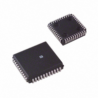
2 ARC MIN PLCC MONO R/D
Manufacturer
Analog Devices Inc
Type
R/D Converterr
Datasheet
1.AD2S80AJD.pdf
(16 pages)
Specifications of AD2S82ALPZ
Rohs Compliant
YES
Input Type
Parallel
Output Type
Digital
Interface
Parallel
Current - Supply
30mA
Mounting Type
Surface Mount
Package / Case
44-PLCC
Lead Free Status / RoHS Status
Lead free / RoHS Compliant
Available stocks
Company
Part Number
Manufacturer
Quantity
Price
Company:

Part Number:
AD2S82ALPZ
Manufacturer:
MAXIM
Quantity:
9 739
Company:
Part Number:
AD2S82ALPZ
Manufacturer:
Analog Devices Inc
Quantity:
10 000
Part Number:
AD2S82ALPZ
Manufacturer:
ADI/亚德诺
Quantity:
20 000


AD2S80A
CONNECTING THE RESOLVER
The recommended connection circuit is shown in Figure 7.
In cases where the reference phase relative to the input signals
from the resolver requires adjustment, this can be easily
achieved by varying the value of the resistor R2 of the HF filter
(see Figure 1).
Assuming that R1 = R2 = R and C1 = C2 = C
and Reference Frequency =
by altering the value of R2, the phase of the reference relative to
the input signals will change in an approximately linear manner
for phase shifts of up to 10 degrees.
Increasing R2 by 10% introduces a phase lag of 2 degrees.
Decreasing R2 by 10% introduces a phase lead of 2 degrees.
PHASE LEAD = ARC TAN
C
R
2 fRC
1
R2
R1
S2
2 π RC
RESOLVER
1
PHASE LAG = ARC TAN 2 fRC
TWISTED PAIR SCREENED CABLE
S4
S3
S1
R
C
TYPICAL CIRCUIT CONFIGURATION
Figure 8 shows a typical circuit configuration for the AD2S80A
in a 12-bit resolution mode. Values of the external components
have been chosen for a reference frequency of 5 kHz and a
maximum tracking rate of 260 rps with a bandwidth of 520 Hz.
Placing the values for R4, R6, C4 and C5 in the equation for K
gives a value of 1.67 × 10
ance preferred values. The capacitors are 100 V ceramic, 10%
tolerance components.
For signal and reference voltages greater than 2 V rms a simple
voltage divider circuit of resistors can be used to generate the
correct signal level at the converter. Care should be taken to
ensure that the ratios of the resistors between the sine signal line
and ground and the cosine signal line and ground are the same.
Any difference will result in an additional position error.
For more information on resistive scaling of SIN, COS and
REFERENCE converter inputs refer to the application note,
“Circuit Applications of the 2S81 and 2S81 Resolver-to-Digital
Converters.”
RELIABILITY
The AD2S80A Mean Time Between Failures (MTBF) has been
calculated according to MIL-HDBK-217E, Figure 10 shows the
MTBF in hours in naval sheltered conditions for AD2S80A/
883B only.
POWER RETURN
C3
R3
(e.g., OSC1758)
OSCILLATOR
1
2
3
4
5
6
7
REF I/P
COS I/P
SIN I/P
ANALOG
GND
SIGNAL
GND
AD2S80A
6
. The resistors are 0.125 W, 5% toler-
DIGITAL
GND
31
A
Related parts for AD2S82ALPZ
Image
Part Number
Description
Manufacturer
Datasheet
Request
R

Part Number:
Description:
±1.7g Dual-Axis IMEMS Accelerometer Evaluation Board
Manufacturer:
Analog Devices Inc
Datasheet:

Part Number:
Description:
Inertial Sensor Evaluation System
Manufacturer:
Analog Devices Inc
Datasheet:
Part Number:
Description:
Manufacturer:
Analog Devices Inc
Datasheet:
Part Number:
Description:
Manufacturer:
Analog Devices Inc
Datasheet:
Part Number:
Description:
Manufacturer:
Analog Devices Inc
Datasheet:
Part Number:
Description:
Manufacturer:
Analog Devices Inc
Datasheet:
Part Number:
Description:
Manufacturer:
Analog Devices Inc
Datasheet:
Part Number:
Description:
Manufacturer:
Analog Devices Inc
Datasheet:
Part Number:
Description:
Manufacturer:
Analog Devices Inc
Datasheet:
Part Number:
Description:
Manufacturer:
Analog Devices Inc
Datasheet:
Part Number:
Description:
Manufacturer:
Analog Devices Inc
Datasheet:
Part Number:
Description:
Manufacturer:
Analog Devices Inc
Datasheet:
Part Number:
Description:
Manufacturer:
Analog Devices Inc
Datasheet: