AD2S82ALPZ Analog Devices Inc, AD2S82ALPZ Datasheet - Page 8
AD2S82ALPZ
Manufacturer Part Number
AD2S82ALPZ
Description
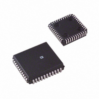
2 ARC MIN PLCC MONO R/D
Manufacturer
Analog Devices Inc
Type
R/D Converterr
Datasheet
1.AD2S80AJD.pdf
(16 pages)
Specifications of AD2S82ALPZ
Rohs Compliant
YES
Input Type
Parallel
Output Type
Digital
Interface
Parallel
Current - Supply
30mA
Mounting Type
Surface Mount
Package / Case
44-PLCC
Lead Free Status / RoHS Status
Lead free / RoHS Compliant
Available stocks
Company
Part Number
Manufacturer
Quantity
Price
Company:

Part Number:
AD2S82ALPZ
Manufacturer:
MAXIM
Quantity:
9 739
Company:
Part Number:
AD2S82ALPZ
Manufacturer:
Analog Devices Inc
Quantity:
10 000
Part Number:
AD2S82ALPZ
Manufacturer:
ADI/亚德诺
Quantity:
20 000


AD2S80A
COMPONENT SELECTION
The following instructions describe how to select the external
components for the converter in order to achieve the required
bandwidth and tracking rate. In all cases the nearest “preferred
value” component should be used, and a 5% tolerance will not
degrade the overall performance of the converter. Care should
be taken that the resistors and capacitors will function over the
required operating temperature range. The components should
be connected as shown in Figure 1.
PG compatible software is available to help users select the optimum
component values for the AD2S80A, and display the transfer gain,
phase and small step response.
For more detailed information and explanation, see section “CIR-
CUIT FUNCTIONS AND DYNAMIC PERFORMANCE.”
1. HF Filter (R1, R2, C1, C2)
2. Gain Scaling Resistor (R4)
3. AC Coupling of Reference Input (R3, C3)
Values should be chosen so that
This filter gives an attenuation of three times at the input to
The function of the HF filter is to remove any dc offset and
to reduce the amount of noise present on the signal inputs to
the AD2S80A, reaching the Phase Sensitive Detector and
affecting the outputs. R1 and C2 may be omitted—in which
case R2 = R3 and C1 = C3, calculated below—but their use
is particularly recommended if noise from switch mode power
supplies and brushless motor drive is present.
and f
the phase sensitive detector.
If R1, C2 are used:
where 100 × 10
If R1, C2 are not used:
where E
Select R3 and C3 so that there is no significant phase shift at
the reference frequency. That is,
with R3 in Ω.
REF
DC
= Reference frequency
C
C
= 160 × 10
= 40 × 10
= 10 × 10
= 2.5 × 10
= Scaling of the DC ERROR in volts
1
1
=
=
–9
C
C
2 15
2
= current/LSB
R4 =
=
=
2
–3
–3
–3
π
–3
C 3 >
R3 = 100 kΩ
100 ×10
R4 =
k
for 12 bits
for 14 bits
for 16 bits
R f
for 10 bits resolution
Ω ≤
1
1
E
DC
REF
100 × 10
R3 × f
R
1
–9
E
=
1
×
DC
R
REF
1
3
2 56
Ω
≤
–9
Ω
F
k
Ω
(Hz)
4. Maximum Tracking Rate (R6)
5. Closed-Loop Bandwidth Selection (C4, C5, R5)
6. VCO Phase Compensation
7. Offset Adjust
where n = bits per revolution
The VCO input resistor R6 sets the maximum tracking rate
of the converter and hence the velocity scaling as at the max
tracking rate, the velocity output will be 8 V.
Decide on your maximum tracking rate, “T,” in revolutions
per second. Note that “T” must not exceed the maximum
tracking rate or 1/16 of the reference frequency.
a. Choose the closed-loop bandwidth (f
Resolution
Typical values may be 100 Hz for a 400 Hz reference frequency
and 500 Hz to 1000 Hz for a 5 kHz reference frequency.
b. Select C4 so that
with R6 in Ω and f
c. C5 is given by
d. R5 is given by
The following values of C6 and R7 should be fitted.
Offsets and bias currents at the integrator input can cause an
additional positional offset at the output of the converter of
1 arc minute typical, 5.3 arc minutes maximum. If this can be
tolerated, then R8 and R9 can be omitted from the circuit.
If fitted, the following values of R8 and R9 should be used:
To adjust the zero offset, ensure the resolver is disconnected
and all the external components are fitted. Connect the COS
pin to the REFERENCE INPUT and the SIN pin to the
SIGNAL GROUND and with the power and reference
applied, adjust the potentiometer to give all “0s” on the
digital output bits.
The potentiometer may be replaced with select on test resistors
if preferred.
ensuring that the ratio of reference frequency to band-
width does not exceed the following guidelines:
10
12
14
16
= 1,024 for 10 bits resolution
= 4,096 for 12 bits
= 16,384 for 14 bits
= 65,536 for 16 bits
R8 = 4.7 MΩ, R9 = 1 MΩ potentiometer
C6 = 470 pF, R7 = 68 Ω
Ratio of Reference Frequency/Bandwidth
BW
R5 =
R6 =
, in Hz selected above.
C4 =
2 × π × f
6. 32 × 10
7.5
C5 = 5 × C4
T × n
2.5 : 1
4
6
R6 × f
4
: 1
: 1
: 1
21
BW
10
BW
Ω
× C5
2
BW
F
) required
Ω
Related parts for AD2S82ALPZ
Image
Part Number
Description
Manufacturer
Datasheet
Request
R

Part Number:
Description:
±1.7g Dual-Axis IMEMS Accelerometer Evaluation Board
Manufacturer:
Analog Devices Inc
Datasheet:

Part Number:
Description:
Inertial Sensor Evaluation System
Manufacturer:
Analog Devices Inc
Datasheet:
Part Number:
Description:
Manufacturer:
Analog Devices Inc
Datasheet:
Part Number:
Description:
Manufacturer:
Analog Devices Inc
Datasheet:
Part Number:
Description:
Manufacturer:
Analog Devices Inc
Datasheet:
Part Number:
Description:
Manufacturer:
Analog Devices Inc
Datasheet:
Part Number:
Description:
Manufacturer:
Analog Devices Inc
Datasheet:
Part Number:
Description:
Manufacturer:
Analog Devices Inc
Datasheet:
Part Number:
Description:
Manufacturer:
Analog Devices Inc
Datasheet:
Part Number:
Description:
Manufacturer:
Analog Devices Inc
Datasheet:
Part Number:
Description:
Manufacturer:
Analog Devices Inc
Datasheet:
Part Number:
Description:
Manufacturer:
Analog Devices Inc
Datasheet:
Part Number:
Description:
Manufacturer:
Analog Devices Inc
Datasheet: