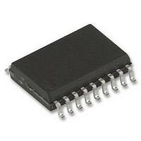
ST62T15CM6 STMicroelectronics, ST62T15CM6 Datasheet - Page 64

ST62T15CM6
Manufacturer Part Number
ST62T15CM6
Description
8BIT MCU OTP 2K, SMD, 62T15, SOIC20
Manufacturer
STMicroelectronics
Datasheet
1.ST62T15CB6.pdf
(105 pages)
Specifications of ST62T15CM6
Controller Family/series
ST6
Core Size
8bit
No. Of I/o's
20
Program Memory Size
2KB
Ram Memory Size
64Byte
Cpu Speed
8MHz
Oscillator Type
External Only
No. Of Timers
1
Digital Ic Case
RoHS Compliant
Peripherals
ADC,
Rohs Compliant
No
Processor Series
ST62T1x
Core
ST6
Data Bus Width
8 bit
Program Memory Type
EPROM
Data Ram Size
64 B
Maximum Clock Frequency
8 MHz
Number Of Programmable I/os
20
Number Of Timers
2
Operating Supply Voltage
3 V to 6 V
Maximum Operating Temperature
+ 85 C
Mounting Style
SMD/SMT
Package / Case
SOP-28
Development Tools By Supplier
ST62GP-EMU2, ST62E2XC-EPB/110, ST62E6XC-EPB/US, STREALIZER-II
Minimum Operating Temperature
- 40 C
On-chip Adc
8 bit
Lead Free Status / Rohs Status
In Transition
Available stocks
Company
Part Number
Manufacturer
Quantity
Price
Company:
Part Number:
ST62T15CM6
Manufacturer:
STM
Quantity:
2 508
Part Number:
ST62T15CM6
Manufacturer:
ST
Quantity:
20 000
ST6215C/ST6225C
11.2 ABSOLUTE MAXIMUM RATINGS
Stresses above those listed as “absolute maxi-
mum ratings” may cause permanent damage to
the device. This is a stress rating only and func-
tional operation of the device under these condi-
11.2.1 Voltage Characteristics
11.2.2 Current Characteristics
11.2.3 Thermal Characteristics
Notes:
1. Directly connecting the RESET and I/O pins to V
2. When the current limitation is not possible, the V
3. Power (V
4. Negative injection disturbs the analog performance of the device. In particular, it induces leakage currents throughout
64/105
1
is generated or an unexpected change of the I/O configuration occurs (for example, due to a corrupted program coun-
ter). To guarantee safe operation, this connection has to be done through a pull-up or pull-down resistor (typical: 4.7k
for RESET, 10k
figuration.
I
the device including the analog inputs. To avoid undesirable effects on the analog functions, care must be taken:
- Analog input pins must have a negative injection less than 1mA (assuming that the impedance of the analog voltage
is lower than the specified limits).
- Pure digital pins must have a negative injection less than 1mA. In addition, it is recommended to inject the current as
far as possible from the analog input pins.
INJ(PIN)
I
INJ(PIN)
V
V
Symbol
Symbol
Symbol
ESD(HBM)
DD
V
T
I
I
specification. A positive injection is induced by V
V
VDD
VSS
I
OUT
STG
T
DD
IO
- V
IN
J
2) & 4)
) and ground (V
SS
for I/Os). Unused I/O pins must be tied in the same way to V
Supply voltage
Input voltage on any pin
Output voltage on any pin
Electro-static discharge voltage (Human Body Model)
Total current into V
Total current out of V
Output current sunk by any standard I/O and control pin
Output current sunk by any high sink I/O pin
Output current source by any I/Os and control pin
Injected current on RESET pin
Injected current on any other pin
Storage temperature range
Maximum junction temperature
(see THERMAL CHARACTERISTICS
SS
) lines must always be connected to the external supply.
DD
SS
power lines (source)
Ratings
Ratings
Ratings
ground lines (sink)
1) & 2)
DD
IN
1) & 2)
or V
absolute maximum rating must be respected, otherwise refer to
SS
IN
>V
could damage the device if an unintentional internal reset
tions is not implied. Exposure to maximum rating
conditions for extended periods may affect device
reliability.
DD
section)
while a negative injection is induced by V
3)
3)
DD
or V
V
V
Maximum value
Maximum value
SS
SS
SS
-0.3 to V
-0.3 to V
-60 to +150
according to their reset con-
Value
3500
100
80
20
40
15
7
5
5
DD
DD
+0.3
+0.3
IN
<V
Unit
Unit
Unit
mA
°C
V
SS
.


