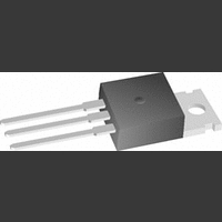
SUM110N04-04-T1-E3 Vishay, SUM110N04-04-T1-E3 Datasheet

SUM110N04-04-T1-E3
Specifications of SUM110N04-04-T1-E3
Related parts for SUM110N04-04-T1-E3
SUM110N04-04-T1-E3 Summary of contents
Page 1
... UNLESS OTHERWISE NOTED) C Symbol 25_C 125_C 0 25_C (TO-220AB and TO-263 25_C (TO-263 Symbol d PCB Mount (TO-263 thJA Free Air (TO-220AB) R thJC SUP/SUB85N04-04 Vishay Siliconix N-Channel MOSFET Limit 240 70 211 c 250 D D 3.75 −55 to 175 stg Limit 40 62.5 0.6 Unit Unit _C/W C/W www.vishay.com 1 ...
Page 2
... SUP/SUB85N04-04 Vishay Siliconix SPECIFICATIONS (T =25_C UNLESS OTHERWISE NOTED) J Parameter Static Drain-Source Breakdown Voltage Gate-Threshold Voltage Gate-Body Leakage Zero Gate Voltage Drain Current g a On-State Drain Current a Drain-Source On-State Resistance a Forward Transconductance b Dynamic Input Capacitance Output Capacitance Reverse Transfer Capacitance c Total Gate Charge ...
Page 3
... Drain-to-Source Voltage (V) DS Document Number: 71125 S-41261—Rev. C, 05-Jul- 0.005 = −55_C C 0.004 25_C 0.003 125_C 0.002 0.001 0.000 80 100 120 32 40 SUP/SUB85N04-04 Vishay Siliconix Transfer Characteristics 250 200 150 100 T = 125_C C 50 25_C − Gate-to-Source Voltage (V) GS On-Resistance vs. Drain Current ...
Page 4
... SUP/SUB85N04-04 Vishay Siliconix TYPICAL CHARACTERISTICS (25_C UNLESS NOTED) On-Resistance vs. Junction Temperature 2 1.6 1.2 0.8 0.4 0.0 −50 − − Junction Temperature (_C) J Avalanche Current vs. Time 1000 100 150_C 0.1 0.00001 0.0001 0.001 0.01 t (Sec) in www.vishay.com 4 100 10 1 100 125 150 175 ...
Page 5
... Document Number: 71125 S-41261—Rev. C, 05-Jul-04 1000 100 10 1 0.1 125 150 175 Normalized Thermal Transient Impedance, Junction-to-Case −2 − Square Wave Pulse Duration (sec) SUP/SUB85N04-04 Vishay Siliconix Safe Operating Area Limited by r DS(on 25_C C Single Pulse 0 − Drain-to-Source Voltage ( 100 ms ...
Page 6
... Vishay disclaims any and all liability arising out of the use or application of any product described herein or of any information provided herein to the maximum extent permitted by law. The product specifications do not expand or otherwise modify Vishay’ ...


