AD9910/PCBZ Analog Devices Inc, AD9910/PCBZ Datasheet - Page 3
AD9910/PCBZ
Manufacturer Part Number
AD9910/PCBZ
Description
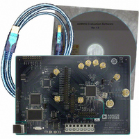
Direct Digital Synthesis Evaluation Board
Manufacturer
Analog Devices Inc
Series
AgileRF™r
Specifications of AD9910/PCBZ
Silicon Manufacturer
Analog Devices
Application Sub Type
Direct Digital Synthesizer
Kit Application Type
Clock & Timing
Silicon Core Number
AD9910
Kit Contents
Board
Design Resources
Synchronizing Multiple AD9910 1 GSPS Direct Digital Synthesizers (CN0121)
Main Purpose
Timing, Direct Digital Synthesis (DDS)
Embedded
No
Utilized Ic / Part
AD9910
Primary Attributes
14-Bit DAC, 32-Bit Tuning Word Width
Secondary Attributes
1GHz, Graphical User Interface
Lead Free Status / RoHS Status
Lead free / RoHS Compliant
Lead Free Status / RoHS Status
Lead free / RoHS Compliant, Lead free / RoHS Compliant
Other names
Q3335404


EVALUATION BOARD HARDWARE
REQUIREMENTS
To successfully use the evaluation board and run the software,
the requirements listed in Table 1 must be met.
Table 1. AD9910/PCBZ Requirements
Item
Operating
Processor
Memory
Ports
Clocking
Power Supplies
Measurement
Cables
SETTING UP THE EVALUATION BOARD
DC Power Supply
The AD9910 evaluation board has two power supply connectors
(four pins each): TB1 and TB2. TB1 powers the USB interface
circuitry, the digital I/O interface, and the digital core. TB2
powers the DAC and the clock input circuitry.
CONNECTORS
Table 2 shows the necessary connections and the appropriate
biasing voltage.
Table 2. Connections and Biasing Voltage
Connector
TB1
TB1
TB1
TB1
TB2
TB2
TB2
System
Requirement
Windows® 98/ME/2000/XP
Pentium® I or later
128 MB minimum
One USB port
Signal generator capable of generating
sinusoidal waves of at least 0 dBm, up to at
least 10 MHz
Capability to generate at least two
independent dc voltages (1.8 V/3.3 V)
Appropriate measurement device, such as a
spectrum analyzer or a high bandwidth
oscilloscope
USB 1.1/2.0 cable, and SMA-to-X cables (X =
SMA or BNC, depending on the connector of
the device interfacing with the board)
Pin No.
1
2
3
4
1, 3
2
4
Label
VCC_USB
GND
DVDD_IO
DVDD
GND
DAC_VDD
CLK_VDD
Voltage (V)
3.3
0
3.3
1.8
0
3.3
1.8
Rev. 0 | Page 3 of 20
Device Clock Oscillator Options
The AD9910 architecture provides the user with three options
when providing an input signal to the part. The first option allows
the user to provide a high frequency input signal, connected to J1.
The second option allows the user to connect using a lower input
reference frequency, enabling the clock multiplier, and connects
through J1. The third option allows the user to connect a crystal
resonator on the backside of the board.
To enable the crystal mode, switch the jumper, W7, to the XTAL
mode. Remove C51 and 52. Place 0 (zero) Ω resistors at R4 and
R11 on the backside of the board. The crystal oscillates at 25 MHz.
Refer to the AD9910 data sheet for details on the maximum input
speeds and input sensitivities of these two inputs.
Device Communication Requirements
Two interface options are available on the evaluation board.
•
•
Analog Devices provides a GUI for the PC; it does not provide
control software for external controllers.
JUMPERS
Use the jumper settings listed in Table 3 to enable different
modes of communication.
Table 3. Jumper Settings for Communication Modes
Mode
PC Control,
USB Port
External
Control
Jumper W1, Jumper W2, and Jumper W4 enable the USB
circuitry to control the AD9910. Jumper W3 controls the
EEPROM, used in starting up the USB circuitry. Jumper W5
and Jumper W6 control Signal SDO and Signal SDIO to and
from the AD9910.
USB 1.1/2.0
Header row (U5 and U9), which places the part under the
control of an external controller (such as a microprocessor,
FPGA, or DSP)
Settings
Set Jumper W1and Jumper W2 to enable. Set
Jumper W4 to enable. Place a jumper on W5, W6,
and W3.
Set Jumper W1and Jumper W2 to disable. Set
Jumper W4 to disable. Remove the jumper on
W5, W6, and W3.
AD9910/PCBZ
Related parts for AD9910/PCBZ
Image
Part Number
Description
Manufacturer
Datasheet
Request
R


Part Number:
Description:
±1.7g Dual-Axis IMEMS Accelerometer Evaluation Board
Manufacturer:
Analog Devices Inc
Datasheet:

Part Number:
Description:
Inertial Sensor Evaluation System
Manufacturer:
Analog Devices Inc
Datasheet:
Part Number:
Description:
Manufacturer:
Analog Devices Inc
Datasheet:
Part Number:
Description:
Manufacturer:
Analog Devices Inc
Datasheet:
Part Number:
Description:
Manufacturer:
Analog Devices Inc
Datasheet:
Part Number:
Description:
Manufacturer:
Analog Devices Inc
Datasheet:
Part Number:
Description:
Manufacturer:
Analog Devices Inc
Datasheet:
Part Number:
Description:
Manufacturer:
Analog Devices Inc
Datasheet:
Part Number:
Description:
Manufacturer:
Analog Devices Inc
Datasheet:
Part Number:
Description:
Manufacturer:
Analog Devices Inc
Datasheet:
Part Number:
Description:
Manufacturer:
Analog Devices Inc
Datasheet:
Part Number:
Description:
Manufacturer:
Analog Devices Inc
Datasheet: