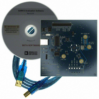
AD9913/PCBZ Analog Devices Inc, AD9913/PCBZ Datasheet - Page 19

AD9913/PCBZ
Manufacturer Part Number
AD9913/PCBZ
Description
Eval Board
Manufacturer
Analog Devices Inc
Series
AgileRF™r
Datasheet
1.AD9913BCPZ.pdf
(32 pages)
Specifications of AD9913/PCBZ
Silicon Manufacturer
Analog Devices
Application Sub Type
Direct Digital Synthesizer
Kit Application Type
Clock & Timing
Silicon Core Number
AD9913
Kit Contents
Board
Tool / Board Applications
D/A Converter
Main Purpose
Timing, Direct Digital Synthesis (DDS)
Embedded
No
Utilized Ic / Part
AD9913
Primary Attributes
10-Bit DAC, 32-Bit Tuning Word Width
Secondary Attributes
250MHz, Graphical User Interface
Lead Free Status / RoHS Status
Lead free / RoHS Compliant
is to reset digital logic in the PLL circuit with an active low
signal. The function of CFR2 [5] is to power up or power down
the PLL.
CFR2 [4] is the PLL LO range bit. When operating the AD9913
with the PLL enabled, CFR2 [4] adjusts PLL loop filter
components to allow low frequency reference clock inputs.
CFR2 [3] enables a divide-by-two circuit at the input of the PLL
phase detector. If this bit is enabled the reference clock signal is
divided by 2 prior to multiplication in the PLL. Refer to the
electrical specifications for the maximum reference clock input
frequency when utilizing the PLL with the divide by 2 circuit
enabled. If the divide by 2 circuit is disabled and the PLL is
enabled, then the maximum reference clock input frequency is
one-half the maximum rate indicated in the electrical
specifications table for the maximum input divider frequency.
The AD9913 PLL uses one of two VCOs for producing the
system clock signal. CFR2 Bit 2 is a select bit that enables an
alternative VCO in the PLL. The basic operation of the PLL is
not affected by the state of this bit. The purpose of offering two
VCOs is to provide performance options. The two VCOs have
approximately the same gain characteristics, but differ in other
aspects. The overall spurious performance, phase noise, and
power consumption may change based on the setting of CFR2
Bit 2. It is important to consider that for either VCO, the
minimum oscillation frequency must be satisfied, and that
minimum oscillation frequency is significantly different
between the two oscillators.
CFR2 [15:9], along with CFR2 [3], determine the multiplication
of the PLL. CFR2 [15] enables a divider at the output of the
Rev. A | Page 19 of 32
PLL. The bits CFR [14:9] control the feedback divider. The
feedback divider is composed of two stages: ÷ N (1:31) selected
by CFR2 [13:9]; ÷ 1 or ÷ 2 selected by CFR2 [14].
Note that the same system clock frequency can be obtained with
different combinations of CFR2 [15:9] and CFR2 [3]. One
combination may work better in a given application either to
run at lower power or to satisfy the VCOs minimum oscillation
frequency
Note that the AD9913 maximum system clock frequency is
250 MHz. If the user intends to use high values for the PLL
feedback divider ratio, then care should be taken that the
system clock frequency does not exceed 250 MHz.
PLL LOCK INDICATION
CFR2 [0] is a read-only bit that displays the status of the PLL
lock signal.
When the AD9913 is programmed to use the PLL, there is some
amount of time required for the loop to lock. While the loop is
not locked, the chip system clock operates at the reference clock
frequency presented to the part at the pins. Once the PLL lock
signal goes high, the system clock frequency switches
asynchronously to operate at the PLL output frequency. To
maintain a system clock frequency with or without a locked
loop if the PLL lock signal transistions low, the chip reverts to
the reference clock signal while the loop attempts to acquire
lock once again.
Table 7 describes how to configure the PLL multiplication factor
using the appropriated register bits.
AD9913


