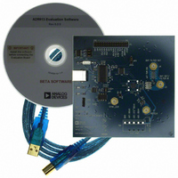
AD9913/PCBZ Analog Devices Inc, AD9913/PCBZ Datasheet - Page 26
AD9913/PCBZ
Manufacturer Part Number
AD9913/PCBZ
Description
Eval Board
Manufacturer
Analog Devices Inc
Series
AgileRF™r
Datasheet
1.AD9913BCPZ.pdf
(32 pages)
Specifications of AD9913/PCBZ
Silicon Manufacturer
Analog Devices
Application Sub Type
Direct Digital Synthesizer
Kit Application Type
Clock & Timing
Silicon Core Number
AD9913
Kit Contents
Board
Tool / Board Applications
D/A Converter
Main Purpose
Timing, Direct Digital Synthesis (DDS)
Embedded
No
Utilized Ic / Part
AD9913
Primary Attributes
10-Bit DAC, 32-Bit Tuning Word Width
Secondary Attributes
250MHz, Graphical User Interface
Lead Free Status / RoHS Status
Lead free / RoHS Compliant


AD9913
REGISTER MAP AND BIT DESCRIPTIONS
REGISTER MAP
Note that the highest number found in the Serial Bit Range column for each register in the following tables is the MSB and the lowest
number is the LSB for that register.
Table 9. Control Registers
Register
Name
(Serial
Address)
CFR1—
Control
Function
Register 1
(0x00)
CFR2—
Control
Function
Register 2
(0x01)
DAC Control
Register
(0x02)
FTW
(0x03)
POW
(0x04)
Linear Sweep
Parameter
Register
(0x06)
Linear Sweep
Delta
Parameter
Register
(0x07)
[Serial Bit
Range]/
Parallel
Address
[7:0]/0x00
[15:8]/0x01
[23:16]/0x02
[31:24]/0x03
[7:0]/0x04
[15:8]/0x05
[7:0]/0x06
[15:8]/0x07
[23:16]/0x08
[31:24]/0x09
[7:0]/0x0A
[15:8]/0x0B
[23:16]/0x0C
[31:24]/0x0D
[7:0]/0x0E
[15:8]/0x0F
[7:0]/0x12
[15:8]/0x13
[23:16]/0x14
[31:24]/0x15
[39:32]/0x16
[47:40]/0x17
[55:48]/0x18
[63:56]/0x19
[7:0]/0x1A
[15:8]/0x1B
[23:16]/0x1C
[31:24]/0x1D
[39:32]/0x1E
[47:40]/0x1F
[55:48]/0x20
[63:56]/0x21
MSB
Bit 7
External
Power-
Down
Mode
Clear
Auxiliary
Accum.
LSB First
Open
CMOS
Clock
Mode
PLL
Output
Div by 2
Open
1
Open [1:0]
Bit 6
Digital
Power-
Down
Clear
Phase
Accum.
Open
Crystal
Clock
Mode
Open
Internal Profile Control [2:0]
1
Bit 5
DAC
Power-
Down
Open
PLL
Power-
Down
00: Frequency Word
Destination [1:0]
01: Phase Word
Rev. A | Page 26 of 32
1
Bit 4
Clock
Input
Power-
Down
Modulus
Enable
PLL LO
Range
Sweep Parameter Word 0 [23:16]
Sweep Parameter Word 0 [31:24]
Sweep Parameter Word 1 [23:16]
Sweep Parameter Word 1 [31:24]
Frequency Tuning Word [23:16]
Frequency Tuning Word [31:24]
Sweep Parameter Word 0 [15:8]
Sweep Parameter Word 1 [15:8]
Frequency Tuning Word [15:8]
Sweep Parameter Word 0 [7:0]
Sweep Parameter Word 1 [7:0]
PLL Multiplication Factor [5:0]
Frequency Tuning Word [7:0]
Falling Delta Word [23:16]
Falling Delta Word [31:24]
Reserved
Rising Delta Word [23:16]
Rising Delta Word [31:24]
Falling Delta Word [15:8]
Rising Delta Word [15:8]
Falling Delta Word [7:0]
Phase Offset Word [7:0]
Rising Delta Word [7:0]
FS C [7:0]
Reserved
Reserved
Bit 3
Load SRR @
IO_UPDATE
Auxiliary
Accumulator
Enable
Sync Clock
Disable
Use Internal
Profile
PLL Input
Div by 2
Phase Offset Word [13:8]
Bit 2
Autoclear
Auxiliary
Accum.
DC
Output
Active
Open
Match
Pipe
Delays
Active
VCO2 Sel
Open
Bit 1
Autoclear
Phase
Accum.
Linear
Sweep
State
Trigger
Active
Open
Open
PLL Reset
FSC [9:8]
LSB
Bit 0
Enable
Sine
Output
Linear
Sweep
No-Dwell
Active
Direct
Switch
Mode
Active
Open
PLL Lock
Open
Default
Value
0x00
0x00
0x00
0x00
0x32
0x14
0xFF
0x13
0x7F
0x00
0x00
0x00
0x00
0x00
0x00
0x00
0x00
0x00
0x00
0x00
0x00
0x00
0x00
0x00
0x00
0x00
0x00
0x00
0x00
0x00
0x00
0x00
Related parts for AD9913/PCBZ
Image
Part Number
Description
Manufacturer
Datasheet
Request
R


Part Number:
Description:
±1.7g Dual-Axis IMEMS Accelerometer Evaluation Board
Manufacturer:
Analog Devices Inc
Datasheet:

Part Number:
Description:
Inertial Sensor Evaluation System
Manufacturer:
Analog Devices Inc
Datasheet:
Part Number:
Description:
Manufacturer:
Analog Devices Inc
Datasheet:
Part Number:
Description:
Manufacturer:
Analog Devices Inc
Datasheet:
Part Number:
Description:
Manufacturer:
Analog Devices Inc
Datasheet:
Part Number:
Description:
Manufacturer:
Analog Devices Inc
Datasheet:
Part Number:
Description:
Manufacturer:
Analog Devices Inc
Datasheet:
Part Number:
Description:
Manufacturer:
Analog Devices Inc
Datasheet:
Part Number:
Description:
Manufacturer:
Analog Devices Inc
Datasheet:
Part Number:
Description:
Manufacturer:
Analog Devices Inc
Datasheet:
Part Number:
Description:
Manufacturer:
Analog Devices Inc
Datasheet:
Part Number:
Description:
Manufacturer:
Analog Devices Inc
Datasheet: