AD9913/PCBZ Analog Devices Inc, AD9913/PCBZ Datasheet - Page 29
AD9913/PCBZ
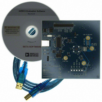
Manufacturer Part Number
AD9913/PCBZ
Description
Eval Board
Manufacturer
Analog Devices Inc
Series
AgileRF™r
Datasheet
1.AD9913BCPZ.pdf
(32 pages)
Specifications of AD9913/PCBZ
Silicon Manufacturer
Analog Devices
Application Sub Type
Direct Digital Synthesizer
Kit Application Type
Clock & Timing
Silicon Core Number
AD9913
Kit Contents
Board
Tool / Board Applications
D/A Converter
Main Purpose
Timing, Direct Digital Synthesis (DDS)
Embedded
No
Utilized Ic / Part
AD9913
Primary Attributes
10-Bit DAC, 32-Bit Tuning Word Width
Secondary Attributes
250MHz, Graphical User Interface
Lead Free Status / RoHS Status
Lead free / RoHS Compliant


Bit(s)
13:12
11
10
9
8
7
6
5
4
3
2
1
0
Bit Name
Destination
Auxiliary Accumulator Enable
DC Output Active
Linear Sweep State Trigger
Active
Linear Sweep No-Dwell Active
External Power-Down Mode
Digital Power-Down
DAC Power-Down
Clock Input Power-Down
LOAD SRR @ IO_UPDATE
Autoclear Auxiliary
Accumulator
Autoclear Phase Accumulator
Enable Sine Output
Description
00 = In direct switch mode, use this setting for FSK.
In linear sweep mode, the auxiliary accumulator is used for frequency sweeping.
In programmable modulus mode, these bits must be 00.
01 = In direct switch mode, use this setting for PSK.
In linear sweep mode, the auxiliary accumulator is used for phase sweeping.
0 = auxiliary accumulator is inactive.
1 = auxiliary accumulator is active.
This bit is ignored if linear sweep is disabled (see CFR1 [11]).
0 = normal operating state.
1 = the output of the DAC is driven to full-scale and the DDS output is disabled.
0 = edge triggered mode active.
1 = state triggered mode active.
This bit is ignored if linear sweep is disabled (see CFR1[11]).
0 = when a sweep is completed, the device holds at the final state.
1 = when a sweep is completed, the device reverts to the initial state.
0 = the external power-down mode selected is the fast recovery power-down mode. In this
mode, when the PWR_DWN_CTL input pin is high, the digital logic and the DAC digital
logic are powered down. The DAC bias circuitry, PLL, oscillator, and clock input circuitry are
not powered down.
1 = the external power-down mode selected is the full power-down mode. In this mode,
when the PWR_DWN_CTL pin is high, all functions are powered down. This includes the
DAC and PLL, which take a significant amount of time to power up.
0 = the digital core is enabled for operation.
1 = the digital core is disabled and is in a low power dissipation state.
0 = the DAC is enabled for operation.
1 = the DAC is disabled and is in its lowest power dissipation state.
0 = normal operation.
1 = shut down all clock generation including the system clock signal going into the digital
section.
0 = every time the linear sweep rate register is updated, the ramp rate timer keeps its
operation until it times out and then loads the update value into the timer.
1 = the timer is interrupted immediately upon the assertion of IO_UPDATE and the value is
loaded.
0 = normal operation.
1 = the auxiliary accumulator is synchronously cleared (zero is loaded) for one cycle upon
receipt of the IO_UPDATE sequence indicator.
0 = normal operation.
1 = the phase accumulator is synchronously cleared for one cycle upon receipt of the
IO_UPDATE sequence indicator.
0 = the angle-to-amplitude conversion logic employs a cosine function.
1 = the angle-to-amplitude conversion logic employs a sine function.
Rev. A | Page 29 of 32
AD9913
Related parts for AD9913/PCBZ
Image
Part Number
Description
Manufacturer
Datasheet
Request
R


Part Number:
Description:
±1.7g Dual-Axis IMEMS Accelerometer Evaluation Board
Manufacturer:
Analog Devices Inc
Datasheet:

Part Number:
Description:
Inertial Sensor Evaluation System
Manufacturer:
Analog Devices Inc
Datasheet:
Part Number:
Description:
Manufacturer:
Analog Devices Inc
Datasheet:
Part Number:
Description:
Manufacturer:
Analog Devices Inc
Datasheet:
Part Number:
Description:
Manufacturer:
Analog Devices Inc
Datasheet:
Part Number:
Description:
Manufacturer:
Analog Devices Inc
Datasheet:
Part Number:
Description:
Manufacturer:
Analog Devices Inc
Datasheet:
Part Number:
Description:
Manufacturer:
Analog Devices Inc
Datasheet:
Part Number:
Description:
Manufacturer:
Analog Devices Inc
Datasheet:
Part Number:
Description:
Manufacturer:
Analog Devices Inc
Datasheet:
Part Number:
Description:
Manufacturer:
Analog Devices Inc
Datasheet:
Part Number:
Description:
Manufacturer:
Analog Devices Inc
Datasheet: