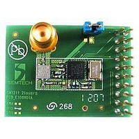
SM1211E915 Semtech, SM1211E915 Datasheet - Page 13

SM1211E915
Manufacturer Part Number
SM1211E915
Description
Dev Kit Accessory
Manufacturer
Semtech
Specifications of SM1211E915
Modulation Type
FSK, OOK
Data Rate Max
200Kbps
Frequency Range
902MHz To 928MHz
Supply Voltage Range
2.1V To 3.6V
Module Interface
SPI
Supply Current
25mA
Accessory Type
RF Module
Sensitivity
-105dBm
Operating Temperature (min)
-40C
Operating Temperature (max)
85C
Operating Temperature Classification
Industrial
Package Type
TQFN EP
Operating Supply Voltage (min)
2.1V
Operating Supply Voltage (typ)
2.5/3.3V
Operating Supply Voltage (max)
3.6V
Sensitivity (dbm)
-105dBm
Rohs Compliant
NA
Lead Free Status / RoHS Status
na
Lead Free Status / RoHS Status
na
To ensure correct operation of the regulator circuit, the decoupling capacitor connection shown in Figure 4 is
required. These decoupling components are recommended for any design.
The frequency synthesizer of the SX1211 is a fully integrated integer-N type PLL. The PLL circuit requires only five
external components for the PLL loop filter and the VCO tank circuit.
The SX1211 embeds a crystal oscillator, which provides the reference frequency for the PLL. The recommended
crystal specification is given in section 7.1.
The reference frequency, or a sub-multiple of it, can be provided on CLKOUT (pin 19) by activating the bit
OSCParam_Clkout_on. The division ratio is programmed through bits OSCParam_Clkout_freq. The two
applications of the CLKOUT output are:
Note: To minimize the current consumption of the SX1211, ensure that the CLKOUT signal is disabled when
unused.
Rev 7 – Sept 2
ADVANCED COMMUNICATIONS & SENSING
3.2. Frequency Synthesis Description
To provide a clock output for a companion uC, thus saving the cost of an additional oscillator. CLKOUT can be
made available in any operation mode, except Sleep mode, and is automatically enabled at power-up.
To provide an oscillator reference output. Measurement of the CLKOUT signal enables simple software
trimming of the initial crystal tolerance.
3.2.1. Reference Oscillator
3.2.2. CLKOUT Output
nd
, 2008
Biasing :
-SPI
-Config. Registers
-POR
Vbat
Y5V
1ųF
Biasing analog
Reg_ana
blocks
1.0 V
Figure 4: Power Supply Breakdown
VR_1V
Pin 27
Y5V
1ųF
220nF
X7R
Page 13 of 92
Biasing digital
Reg_top
blocks
Reg_dig
1.4 V
1.0 V
VR_DIG
External Supply
Pin 28
VDD – Pin 26
2.1 – 3.6V
100nF
X7R
Biasing :
-VCO circuit
-Ext. VCO
tank
Reg_VCO
0.85 V
VR_VCO
Pin 3
47nF
Biasing :
-PA Driver
-PA choke
(ext)
X7R
Reg_PA
1.80 V
VR_PA
Pin 29
www.semtech.com
SX1211


