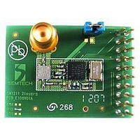
SM1211E915 Semtech, SM1211E915 Datasheet - Page 37

SM1211E915
Manufacturer Part Number
SM1211E915
Description
Dev Kit Accessory
Manufacturer
Semtech
Specifications of SM1211E915
Modulation Type
FSK, OOK
Data Rate Max
200Kbps
Frequency Range
902MHz To 928MHz
Supply Voltage Range
2.1V To 3.6V
Module Interface
SPI
Supply Current
25mA
Accessory Type
RF Module
Sensitivity
-105dBm
Operating Temperature (min)
-40C
Operating Temperature (max)
85C
Operating Temperature Classification
Industrial
Package Type
TQFN EP
Operating Supply Voltage (min)
2.1V
Operating Supply Voltage (typ)
2.5/3.3V
Operating Supply Voltage (max)
3.6V
Sensitivity (dbm)
-105dBm
Rohs Compliant
NA
Lead Free Status / RoHS Status
na
Lead Free Status / RoHS Status
na
Note that when reading more than one register successively, it is not compulsory to toggle NSS_CONFIG back
high between two read sequences. The bytes are alternatively considered as address and value.
To write bytes into the FIFO the timing diagram below should be carefully followed by the uC.
Note that it is compulsory to toggle NSS_DATA back high between each byte written.
The byte is pushed into the FIFO on the rising edge of NSS_DATA
Rev 7 – Sept 2
NSS_CONFIG (In)
SCK (In)
MOSI (In)
MISO (Out)
ADVANCED COMMUNICATIONS & SENSING
Write Byte (before/during Tx)
SCK (In)
MOSI (In)
MISO (Out)
NSS_DATA (In)
HZ
(input)
nd
, 2008
HZ
(input)
5.2.1.3. SPI Data
start
1
x
x
D1(7)
1
rw
D1(6) D1(5) D1(4)
2
x
2
x
A(4) A(3) A(2) A(1)
3
x
3
x
Figure 29: Write Bytes Sequence (ex: 2 bytes)
1
st
4
x
Address = A1
byte written
4
x
x
Figure 28: Read Register Sequence
D1(3) D1(2) D1(1)
5
x
5
x
6
x
6
x
7
x
A(0)
Page 37 of 92
7
D1(0)
x
8
x
stop
8
(input)
x
HZ
D(7) D(6) D(5) D(4) D(3) D(2) D(1)
x
9
D2(7) D2(6) D2(5)
x
1
10
x
2
x
11
x
3
x
Current value at
address A1
2
nd
D2(4)
12
x
4
x
byte written
D2(3) D2(2) D2(1)
5
x
13
x
6
x
14
x
7
x
15
x
D2(0)
8
x
www.semtech.com
SX1211
16
D(0)
x
x
HZ
(input)
HZ
(input)


