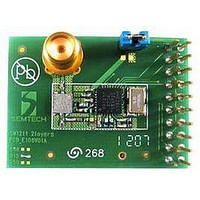
SM1211E915 Semtech, SM1211E915 Datasheet - Page 22

SM1211E915
Manufacturer Part Number
SM1211E915
Description
Dev Kit Accessory
Manufacturer
Semtech
Specifications of SM1211E915
Modulation Type
FSK, OOK
Data Rate Max
200Kbps
Frequency Range
902MHz To 928MHz
Supply Voltage Range
2.1V To 3.6V
Module Interface
SPI
Supply Current
25mA
Accessory Type
RF Module
Sensitivity
-105dBm
Operating Temperature (min)
-40C
Operating Temperature (max)
85C
Operating Temperature Classification
Industrial
Package Type
TQFN EP
Operating Supply Voltage (min)
2.1V
Operating Supply Voltage (typ)
2.5/3.3V
Operating Supply Voltage (max)
3.6V
Sensitivity (dbm)
-105dBm
Rohs Compliant
NA
Lead Free Status / RoHS Status
na
Lead Free Status / RoHS Status
na
The recommended PA bias and matching circuit is illustrated below:
Please refer to section 7.5.3 of this document for the optimized matching arrangement for each frequency band.
The receiver and the transmitter share the same RFIO pin (pin 31). Figure 13 below shows the configuration of the
common RF front-end.
Rev 7 – Sept 2
ADVANCED COMMUNICATIONS & SENSING
In transmit mode, the PA and the PA regulator are active, with the voltage on the VR_PA pin equal to the
nominal voltage of the regulator (1.8 V). The external inductance is used to bias the PA.
In receive mode, both PA and PA regulator are off and VR_PA is tied to ground. The external inductance LT1
is then used to bias the LNA.
3.3.8. Common Input and Output Front-End
nd
, 2008
3.3.7.3. Suggested PA Biasing and Matching
Figure 12: Recommended PA Biasing and Output Matching
PA
To
Antenna
VR_PA
RFIO
Figure 13: Front-end Description
VR_PA
RFIO
100nH
Low-pass and DC block
Page 22 of 92
47nF
Rx_on
Reg_PA
LNA
PA
SAW
DC block
Antenna
port
www.semtech.com
SX1211


