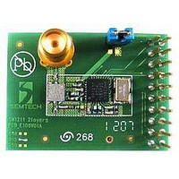
SM1211E915 Semtech, SM1211E915 Datasheet - Page 16

SM1211E915
Manufacturer Part Number
SM1211E915
Description
Dev Kit Accessory
Manufacturer
Semtech
Specifications of SM1211E915
Modulation Type
FSK, OOK
Data Rate Max
200Kbps
Frequency Range
902MHz To 928MHz
Supply Voltage Range
2.1V To 3.6V
Module Interface
SPI
Supply Current
25mA
Accessory Type
RF Module
Sensitivity
-105dBm
Operating Temperature (min)
-40C
Operating Temperature (max)
85C
Operating Temperature Classification
Industrial
Package Type
TQFN EP
Operating Supply Voltage (min)
2.1V
Operating Supply Voltage (typ)
2.5/3.3V
Operating Supply Voltage (max)
3.6V
Sensitivity (dbm)
-105dBm
Rohs Compliant
NA
Lead Free Status / RoHS Status
na
Lead Free Status / RoHS Status
na
Note for mass production: The VCO capacitance is piece to piece dependant. As such, the optimization proposed
above should be verified on several prototypes, to ensure that the population is centered on 100 mV.
To adequately reject spurious components arising from the comparison frequency Fcomp, an external 2
loop filter is employed.
Following the recommendations made in section 3.2.4, the loop filter proposed in the reference design’s bill of
material on section 7.5.3 should be used. The loop filter settings are frequency band independent and are hence
relevant to all implementations of the SX1211.
The SX1211 also features a PLL lock detect indicator. This is useful for optimizing power consumption, by adjusting
the synthesizer wake up time (TS_FS), since the PLL startup time is lower than specified under nominal conditions.
The lock status can be read on bit IRQParam_PLL_lock, and must be cleared by writing a “1” to this same register.
In addition, the lock status can be reflected in pin 23 PLL_LOCK, by setting the bit IRQParam_Enable_lock_detect.
As shown in Figure 5 the PLL structure comprises three different dividers, R, P and S, which set the output
frequency through the LO. A second set of dividers is also available to allow rapid switching between a pair of
frequencies: R1/P1/S1 and R2/P2/S2. These six dividers are programmed by six bytes of the register MCParam
from addresses 6 to 11.
The following formula gives the relationship between the local oscillator, and R, P and S values, when using FSK
modulation.
Due to the manner in which the baseband OOK symbols are generated, the signal is always offset by the FSK
frequency deviation (Fdev - as programmed in MCParam_Freq_dev). Hence, the center of the transmitted OOK
signal is:
Rev 7 – Sept 2
ADVANCED COMMUNICATIONS & SENSING
3.2.6. PLL Loop Filter
3.2.7. PLL Lock Detection Indicator
3.2.8. Frequency Calculation
nd
, 2008
3.2.8.1. FSK Mode
3.2.8.2. OOK Mode
CL2
Frf
Frf
,
,
fsk
fsk
Figure 7: Loop Filter
RL1
9
8
9
8
CL1
Page 16 of 92
Flo
Fxtal
R
1
75
P
LF_M
LF_P
) 1
S
www.semtech.com
SX1211
nd
order


