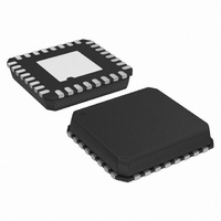
AD7266BCPZ-REEL Analog Devices Inc, AD7266BCPZ-REEL Datasheet - Page 17

AD7266BCPZ-REEL
Manufacturer Part Number
AD7266BCPZ-REEL
Description
IC,Data Acquisition System,6-CHANNEL,12-BIT,LLCC,32PIN,PLASTIC
Manufacturer
Analog Devices Inc
Datasheet
1.AD7266BCPZ-REEL.pdf
(28 pages)
Specifications of AD7266BCPZ-REEL
Design Resources
AD7266 SAR ADC in DC-Coupled Differential and Single-Ended Appls (CN0039)
Number Of Bits
12
Sampling Rate (per Second)
2M
Data Interface
DSP, MICROWIRE™, QSPI™, Serial, SPI™
Number Of Converters
2
Power Dissipation (max)
33.6mW
Voltage Supply Source
Analog and Digital
Operating Temperature
-40°C ~ 125°C
Mounting Type
Surface Mount
Package / Case
32-VFQFN, CSP Exposed Pad
Lead Free Status / RoHS Status
Lead free / RoHS Compliant
For Use With
EVAL-AD7266CBZ - BOARD EVALUATION FOR AD7266
Lead Free Status / RoHS Status
Lead free / RoHS Compliant
ANALOG INPUT SELECTION
The analog inputs of the AD7266 can be configured as single-
ended or true differential via the SGL/ DIFF logic pin, as shown
in Figure 31. If this pin is tied to a logic low, the analog input
channels to each on-chip ADC are set up as three true
differential pairs. If this pin is at logic high, the analog input
channels to each on-chip ADC are set up as six single-ended
analog inputs. The required logic level on this pin needs to be
established prior to the acquisition time and remain unchanged
during the conversion time until the track-and-hold has returned
to track. The track-and-hold returns to track on the 13
edge of SCLK after the CS falling edge (see Figure 41). If the
level on this pin is changed, it will be recognized by the
AD7266; therefore, it is necessary to keep the same logic level
during acquisition and conversion to avoid corrupting the
conversion in progress.
For example, in Figure 31 the SGL/ DIFF
for the duration of both the acquisition and conversion times so
the analog inputs are configured as single ended for that
conversion (Sampling Point A). The logic level of the SGL/
changed to low after the track-and-hold returned to track and
prior to the required acquisition time for the next sampling
instant at Point B; therefore, the analog inputs are configured as
differential for that conversion.
Table 6. Analog Input Type and Channel Selection
SGL/ DIFF
1
1
1
1
1
1
0
0
0
0
0
0
SGL/DIFF
SCLK
CS
Figure 31. Selecting Differential or Single-Ended Configuration
A
1
t
ACQ
A2
0
0
0
0
1
1
0
0
0
0
1
1
14
A1
0
0
1
1
0
0
0
0
1
1
0
0
pin is set at logic high
A0
0
1
0
1
0
1
0
1
0
1
0
1
B
1
V
V
V
V
V
V
V
V
V
V
V
V
V
A1
A2
A3
A4
A5
A6
A1
A1
A3
A3
A5
A5
IN+
14
th
rising
DIFF
ADC A
Rev. A | Page 17 of 28
V
AGND
AGND
AGND
AGND
AGND
AGND
V
V
V
V
V
V
A2
A2
A4
A4
A6
A6
IN−
The channels used for simultaneous conversions are selected via
the multiplexer address input pins, A0 to A2. The logic states of
these pins also need to be established prior to the acquisition
time; however, they may change during the conversion time
provided the mode is not changed. If the mode is changed from
fully differential to pseudo differential, for example, then the
acquisition time would start again from this point. The selected
input channels are decoded as shown in
The analog input range of the AD7266 can be selected as 0 V to
V
made in a similar fashion to that of the SGL/ DIFF pin by setting
the logic state of the RANGE pin a time t
edge of CS . Subsequent to this, the logic level on this pin can be
altered after the third falling edge of SCLK. If this pin is tied to a
logic low, the analog input range selected is 0 V to V
pin is tied to a logic high, the analog input range selected is 0 V
to 2 × V
OUTPUT CODING
The AD7266 output coding is set to either twos complement or
straight binary, depending on which analog input configuration
is selected for a conversion.
scheme is used for each possible analog input configuration.
Table 5. AD7266 Output Coding
SGL/ DIFF
DIFF
DIFF
SGL
SGL
PSEUDO DIFF
PSEUDO DIFF
REF
V
V
V
V
V
V
V
V
V
V
V
V
V
or 0 V to 2 × V
B1
B2
B3
B4
B5
B6
B1
B1
B3
B3
B5
B5
IN+
REF
.
ADC B
V
AGND
AGND
AGND
AGND
AGND
AGND
V
V
V
V
V
V
B2
B2
B4
B4
B6
B6
IN−
REF
Range
0 V to V
0 V to 2 × V
0 V to V
0 V to 2 × V
0 V to V
0 V to 2 × V
via the RANGE pin. This selection is
REF
REF
REF
Table 5 shows which output coding
Comment
Single ended
Single ended
Single ended
Single ended
Single ended
Single ended
Fully differential
Pseudo differential
Fully differential
Pseudo differential
Fully differential
Pseudo differential
REF
REF
REF
Output Coding
Twos complement
Twos complement
Straight binary
Twos complement
Straight binary
Twos complement
Table 6.
acq
prior to the falling
AD7266
REF
. If this


