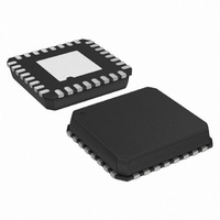
AD7266BCPZ-REEL Analog Devices Inc, AD7266BCPZ-REEL Datasheet - Page 18

AD7266BCPZ-REEL
Manufacturer Part Number
AD7266BCPZ-REEL
Description
IC,Data Acquisition System,6-CHANNEL,12-BIT,LLCC,32PIN,PLASTIC
Manufacturer
Analog Devices Inc
Datasheet
1.AD7266BCPZ-REEL.pdf
(28 pages)
Specifications of AD7266BCPZ-REEL
Design Resources
AD7266 SAR ADC in DC-Coupled Differential and Single-Ended Appls (CN0039)
Number Of Bits
12
Sampling Rate (per Second)
2M
Data Interface
DSP, MICROWIRE™, QSPI™, Serial, SPI™
Number Of Converters
2
Power Dissipation (max)
33.6mW
Voltage Supply Source
Analog and Digital
Operating Temperature
-40°C ~ 125°C
Mounting Type
Surface Mount
Package / Case
32-VFQFN, CSP Exposed Pad
Lead Free Status / RoHS Status
Lead free / RoHS Compliant
For Use With
EVAL-AD7266CBZ - BOARD EVALUATION FOR AD7266
Lead Free Status / RoHS Status
Lead free / RoHS Compliant
AD7266
TRANSFER FUNCTIONS
The designed code transitions occur at successive integer LSB
values (1 LSB, 2 LSB, and so on). In single-ended mode, the LSB
size is V
LSB size is 2 × V /4096 when the 0 V to 2 × V
In differential mode, the LSB size is 2 × V
to V
0 V to 2 × V
for the AD7266 when straight binary coding is output is shown
in
AD7266 when twos complement coding is output is shown in
Figure 33 (this is shown with the 2 × V
Figure 32, and the ideal transfer characteristic for the
NOTE
1. V
REF
REF
011...111
011...110
000...001
000...000
111...111
100...010
100...001
100...000
111...111
111...110
111...000
011...111
000...010
000...001
000...000
range is used, and the LSB size is 4 × V
Figure 33. Twos Complement Transfer Characteristic with
REF
IS EITHER V
/4096 when the 0 V to V
–V
Figure 32. Straight Binary Transfer Characteristic
REF
REF
0V
range is used. The ideal transfer characteristic
1LSB
REF
+ 1LSB V
1LSB = 2
REF
OR 2 × V
V
REF
REF
×
V
± V
REF
– 1LSB
REF
ANALOG INPUT
REF
/4096
.
ANALOG INPUT
Input Range
1LSB = V
+V
REF
REF
range is used, and the
REF
V
REF
– 1 LSB
REF
range).
REF
– 1LSB
/4096 when the 0 V
/4096
REF
REF
/4096 when the
range is used.
Rev. A | Page 18 of 28
DIGITAL INPUTS
The digital inputs applied to the AD7266 are not limited by the
maximum ratings that limit the analog inputs. Instead, the
digital inputs can be applied up to 7 V and are not restricted by
the V
Maximum Ratings
advantage of the SCLK, RANGE, A0 to A2, and
being restricted by the V
sequencing issues are avoided. If one of these digital inputs is
applied before V
be on the analog inputs if a signal greater than 0.3 V were
applied prior to V
V
The AD7266 also has a V
which the serial interface operates. V
easily interface to both 3 V and 5 V processors. For example, if
the AD7266 was operated with a V
could be powered from a 3 V supply, allowing a large dynamic
range with low voltage digital processors. Therefore, the
AD7266 could be used with the 2 × V
of 5 V while still being able to interface to 3 V digital parts.
DRIVE
DD
+ 0.3 V limit as are the analog inputs. See the
DD
DD
, there is no risk of latch-up, as there would
section for more information. Another
.
DD
DRIVE
+ 0.3 V limit is that power supply
feature to control the voltage at
DD
DRIVE
of 5 V, the V
REF
input range, with a V
allows the ADC to
CS pins not
DRIVE
Absolute
pin
DD


