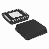
AD7266BCPZ-REEL Analog Devices Inc, AD7266BCPZ-REEL Datasheet - Page 5

AD7266BCPZ-REEL
Manufacturer Part Number
AD7266BCPZ-REEL
Description
IC,Data Acquisition System,6-CHANNEL,12-BIT,LLCC,32PIN,PLASTIC
Manufacturer
Analog Devices Inc
Datasheet
1.AD7266BCPZ-REEL.pdf
(28 pages)
Specifications of AD7266BCPZ-REEL
Design Resources
AD7266 SAR ADC in DC-Coupled Differential and Single-Ended Appls (CN0039)
Number Of Bits
12
Sampling Rate (per Second)
2M
Data Interface
DSP, MICROWIRE™, QSPI™, Serial, SPI™
Number Of Converters
2
Power Dissipation (max)
33.6mW
Voltage Supply Source
Analog and Digital
Operating Temperature
-40°C ~ 125°C
Mounting Type
Surface Mount
Package / Case
32-VFQFN, CSP Exposed Pad
Lead Free Status / RoHS Status
Lead free / RoHS Compliant
For Use With
EVAL-AD7266CBZ - BOARD EVALUATION FOR AD7266
Lead Free Status / RoHS Status
Lead free / RoHS Compliant
TIMING SPECIFICATIONS
AV
Table 2.
Parameter
f
t
t
t
t
t
t
t
t
t
t
t
1
2
3
SCLK
CONVERT
QUIET
2
3
4
5
6
7
8
9
10
Sample tested during initial release to ensure compliance. All input signals are specified with tr = tf = 5 ns (10% to 90% of V
All timing specifications given are with a 25 pF load capacitance. With a load capacitance greater than this value, a digital buffer or latch must be used. See Serial
Interface section and Figure 41 and Figure 42.
Minimum SCLK for specified performance; with slower SCLK frequencies, performance specifications apply typically.
The time required for the output to cross 0.4 V or 2.4 V.
3
DD
2
= DV
DD
= 2.7 V to 5.25 V, V
Limit at T
1
4
32
14 × t
437.5
583.3
30
15/20
20/30
15
36
27
0.45 t
0.45 t
10
5
15
30
5
35
SCLK
SCLK
SCLK
MIN
, T
MAX
DRIVE
= 2.7 V to 5.25 V, internal/external reference = 2.5 V, T
Unit
MHz min
MHz min
MHz max
ns max
ns max
ns max
ns min
ns min
ns min
ns max
ns max
ns max
ns min
ns min
ns min
ns min
ns max
ns min
ns min
ns max
Rev. A | Page 5 of 28
Description
T
T
t
f
f
Minimum time between end of serial read and next falling edge of
V
V
Delay from
Data access time after SCLK falling edge, V
Data access time after SCLK falling edge, V
SCLK low pulse width
SCLK high pulse width
SCLK to data valid hold time, V
SCLK to data valid hold time, V
CS
CS
SCLK falling edge to D
SCLK falling edge to D
SCLK
SCLK
SCLK
A
A
DD
DD
= −40°C to +85°C
> 85°C to 125°C
rising edge to D
rising edge to falling edge pulse width
= 5 V/3 V,
= 5 V /3 V,
= 1/f
= 32 MHz, V
= 24 MHz, V
SCLK
CS
CS
CS
until D
DD
DD
to SCLK setup time, T
to SCLK setup time, T
= 5 V, f
= 3 V, f
OUT
OUT
A, D
OUT
OUT
A and D
A, D
A, D
SAMPLE
SAMPLE
OUT
B, high impedance
OUT
OUT
DD
DD
A
= 2 MSPS
= 1.5 MSPS
B, high impedance
B, high impedance
OUT
= T
= 3 V
= 5 V
B are three-state disabled
MAX
A
A
= −40°C to +85°C
DD
> 85°C to 125°C
to T
) and timed from a voltage level of 1.6 V.
DD
DD
MIN
= 3 V
= 5 V
, unless otherwise noted
AD7266
CS
1
.


