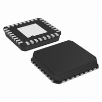
AD7266BCPZ-REEL Analog Devices Inc, AD7266BCPZ-REEL Datasheet - Page 20

AD7266BCPZ-REEL
Manufacturer Part Number
AD7266BCPZ-REEL
Description
IC,Data Acquisition System,6-CHANNEL,12-BIT,LLCC,32PIN,PLASTIC
Manufacturer
Analog Devices Inc
Datasheet
1.AD7266BCPZ-REEL.pdf
(28 pages)
Specifications of AD7266BCPZ-REEL
Design Resources
AD7266 SAR ADC in DC-Coupled Differential and Single-Ended Appls (CN0039)
Number Of Bits
12
Sampling Rate (per Second)
2M
Data Interface
DSP, MICROWIRE™, QSPI™, Serial, SPI™
Number Of Converters
2
Power Dissipation (max)
33.6mW
Voltage Supply Source
Analog and Digital
Operating Temperature
-40°C ~ 125°C
Mounting Type
Surface Mount
Package / Case
32-VFQFN, CSP Exposed Pad
Lead Free Status / RoHS Status
Lead free / RoHS Compliant
For Use With
EVAL-AD7266CBZ - BOARD EVALUATION FOR AD7266
Lead Free Status / RoHS Status
Lead free / RoHS Compliant
AD7266
FULL POWER-DOWN MODE
This mode is intended for use in applications where throughput
rates slower than those in the partial power-down mode are
required, as power-up from a full power-down takes substan-
tially longer than that from partial power-down. This mode is
more suited to applications where a series of conversions
performed at a relatively high throughput rate are followed by a
long period of inactivity and thus power-down. When the
AD7266 is in full power-down, all analog circuitry is powered
down. Full power-down is entered in a similar way as partial
power-down, except the timing sequence shown in
must be executed twice. The conversion process must be
interrupted in a similar fashion by bringing CS high anywhere
after the second falling edge of SCLK and before the 10
edge of SCLK. The device enters partial power-down at this
point. To reach full power-down, the next conversion cycle
must be interrupted in the same way, as shown in Figure 37.
Once CS is brought high in this window of SCLKs, the part
completely powers down.
D
D
D
D
SCLK
SCLK
OUT
OUT
OUT
OUT
CS
CS
A
B
A
B
THE PART BEGINS
TO POWER UP.
1
1
2
INVALID DATA
PARTIAL POWER DOWN.
THE PART ENTERS
INVALID DATA
t
POWER-UP1
Figure 36. Exiting Partial Power-Down Mode
10
Figure 37. Entering Full Power-Down Mode
Figure 35
10
THREE-STATE
th
falling
Rev. A | Page 20 of 28
14
14
THE PART BEGINS
TO POWER UP.
Note that it is not necessary to complete the 14 SCLKs once
is brought high to enter a power-down mode.
To exit full power-down and power up the AD7266, a dummy
conversion is performed, as when powering up from partial
power-down. On the falling edge of CS , the device begins to
power up and continues to power up, as long as CS is held low
until after the falling edge of the 10
power-up time must elapse before a conversion can be initiated,
as shown in Figure 38. See the Power-Up Times section for the
power-up times associated with the AD7266.
1
2
INVALID DATA
1
THE PART IS FULLY
POWERED UP; SEE
POWER-UP TIMES
SECTION.
FULL POWER DOWN.
THE PART ENTERS
VALID DATA
10
THREE-STATE
14
th
SCLK. The required
14
CS


