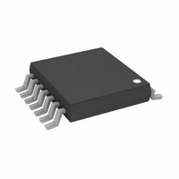
AD8367ARU-REEL7 Analog Devices Inc, AD8367ARU-REEL7 Datasheet - Page 10

AD8367ARU-REEL7
Manufacturer Part Number
AD8367ARU-REEL7
Description
IC,Voltage Controlled Gain Amplifier,SINGLE,TSSOP,14PIN,PLASTIC
Manufacturer
Analog Devices Inc
Series
X-AMP®r
Datasheet
1.AD8367-EVAL.pdf
(24 pages)
Specifications of AD8367ARU-REEL7
Rohs Status
RoHS non-compliant
Amplifier Type
Variable Gain
Number Of Circuits
1
-3db Bandwidth
500MHz
Current - Input Bias
27µA
Current - Supply
26mA
Voltage - Supply, Single/dual (±)
2.7 V ~ 5.5 V
Operating Temperature
-40°C ~ 85°C
Mounting Type
Surface Mount
Package / Case
14-TSSOP
Output Type
-
Current - Output / Channel
-
Slew Rate
-
Gain Bandwidth Product
-
Voltage - Input Offset
-
Lead Free Status / RoHS Status
AD8367
Figure 21. AGC RSSI (Voltage on DETO Pin) vs. Input Power at 10 MHz,
1.0
0.9
0.8
0.7
0.6
0.5
0.4
0.3
0.2
0.1
1.0
0.9
0.8
0.7
0.6
0.5
0.4
0.3
0.2
0.1
1.0
0.9
0.8
0.7
0.6
0.5
0.4
0.3
0.2
0.1
0
0
0
–60
–60
–60
Figure 23. AGC RSSI (Voltage on DETO Pin) vs. Input Power
Figure 22. AGC RSSI (Voltage on DETO Pin) vs.
–50
–50
–50
Input Power over Temperature at 70 MHz
70MHz
–40°C
for Various Modulation Schemes
10MHz
70 MHz, 140 MHz, and 240 MHz
240MHz
–40
INPUT LEVEL (dBV rms)
–40
INPUT LEVEL (dBV rms)
–40
INPUT LEVEL (dBV rms)
+85°C
140MHz
–30
–30
–30
+25°C
–20
–20
256QAM
–20
WCDMA
64QAM
–10
–10
–10
10MHz
70MHz
140MHz
240MHz
IS95FWD
+25°C
–40°C
+85°C
16QAM
SINE
0
0
0
2.0
1.5
1.0
0.5
0
–0.5
–1.0
–1.5
–2.0
–2.5
–3.0
2.0
1.5
1.0
0.5
0
–0.5
–1.0
–1.5
–2.0
–2.5
–3.0
2.5
2.0
1.5
1.0
0.5
0
–0.5
–1.0
–1.5
–2.0
–2.5
Rev. A | Page 10 of 24
19.0097
0.8
0.7
0.6
0.5
0.4
–2
–6.4
–5
Figure 24. AGC Time Domain Response (3 dB Step)
Figure 26. Gain Intercept Distribution at 70 MHz
Figure 25. Gain Scaling Distribution at 70 MHz
–6.2
19.7297
–1
–6.0
–5
GAIN SCALING (mV/dB)
–5.8
INTERCEPT (dB)
TIME (Seconds)
19.9097
C
–5.6
AGC
0
= 100pF
–5.4
V
V
AGC
OUT
20.0897
–5.2
1
–5
–5.0
20.2697
–4.8
2
–5


