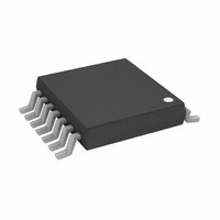
AD8367ARU-REEL7 Analog Devices Inc, AD8367ARU-REEL7 Datasheet - Page 14

AD8367ARU-REEL7
Manufacturer Part Number
AD8367ARU-REEL7
Description
IC,Voltage Controlled Gain Amplifier,SINGLE,TSSOP,14PIN,PLASTIC
Manufacturer
Analog Devices Inc
Series
X-AMP®r
Datasheet
1.AD8367-EVAL.pdf
(24 pages)
Specifications of AD8367ARU-REEL7
Rohs Status
RoHS non-compliant
Amplifier Type
Variable Gain
Number Of Circuits
1
-3db Bandwidth
500MHz
Current - Input Bias
27µA
Current - Supply
26mA
Voltage - Supply, Single/dual (±)
2.7 V ~ 5.5 V
Operating Temperature
-40°C ~ 85°C
Mounting Type
Surface Mount
Package / Case
14-TSSOP
Output Type
-
Current - Output / Channel
-
Slew Rate
-
Gain Bandwidth Product
-
Voltage - Input Offset
-
Lead Free Status / RoHS Status
AD8367
APPLICATIONS
The AD8367 can be configured either as a VGA whose gain
is controlled externally through the GAIN pin or as an AGC
amplifier, using a supply voltage of 2.7 V to 5.5 V. The supply
to the VPSO and VPSI pins should be decoupled using a low
inductance, 0.1 μF surface-mount, ceramic capacitor as close
as possible to the device. Additional supply decoupling can
be provided by a small series resistor. A 10 nF capacitor from
Pin DECL to Pin OCOM is recommended to decouple the
output reference voltage.
INPUT AND OUTPUT MATCHING
The AD8367 is designed to operate in a 200 Ω impedance
system. The output amplifier is a low output impedance voltage
buffer with a 50 Ω damping resistor to desensitize it from load
reactance and parasitics. The quoted performance includes the
voltage division between the 50 Ω resistor and the 200 Ω load.
The AD8367 can be reactively matched to an impedance other
than 200 Ω by using traditional step-up and step down
matching networks or high quality transformers. Table 4 lists
the 50 Ω S-parameters for the AD8367 at a V
Figure 32 illustrates an example where the AD8367 is matched
to 50 Ω at 140 MHz. As shown in the Smith Chart, the input
matching network shifts the input impedance from Z
with an insertion loss of <2 dB over a 5 MHz bandwidth. For
the output network, the 50 Ω load is made to present 200 Ω to
the AD8367 output. Table 5 provides the component values
required for 50 Ω matching at several frequencies of interest.
When added loss and noise can be tolerated, a resistive pad can
be used to provide broadband, near-matched impedances at the
device terminals and the terminations.
Table 4. S-Parameters for 200 Ω System for V
Frequency (MHz)
10
70
140
190
240
Table 5. Reactive Matching Components for a 50 Ω System where R
Frequency (MHz)
10
70
140
190
240
XS
1.5 μH
220 nH
100 nH
82 nH
68 nH
S11
0.04 ∠ −43.8°
0.09 ∠ −81.5°
0.17 ∠ −103.4°
0.21 ∠ −111.7°
0.26 ∠ −103.8°
IN
GAIN
S
= 5 V and V
= 750 mV.
IN
to 50 Ω
XP
120
15
8.2
2.7
1.5
S21
41.1 ∠ 178.8°
43.6 ∠ 163.4°
48.0 ∠ 141.4°
47.5 ∠ 124.0°
48.3 ∠ 107.6°
Rev. A | Page 14 of 24
GAIN
IN
(pF)
= 0.75 V
SOURCE
Minimum-loss, L-pad networks are used on the evaluation
board (see Figure 45) to allow easy interfacing to standard
50 Ω test equipment. Each pad introduces an 11.5 dB power
loss (5.5 dB voltage loss).
R
SOURCE
= 50 Ω, R
–0.3333
V
50Ω
0.3333
S
f
Figure 32. Reactive Matching Example for f = 140 MHz
C
100nH
8.2pF
XS
XP
= 140MHz, Z
XS
180
27
13
10
7
S12
0.0003 ∠ 76.1°
0.0002 ∠ 63.7°
0.0009 ∠ 130.8°
0.0017 ∠ 96.8°
0.0018 ∠ 113.5°
IN
LOAD
IN
OUT
Z
IN
= 50 Ω
(pF)
0.3333
IN
= 197 – j34.2, R
Z
IN
SERIES L
R
SOURCE
AD8367
1
–1
1
SOURCE
Z
OUT
SHUNT C
S22
0.56 ∠ −179.3°
0.55 ∠ +176.1°
0.56 ∠ +170.2°
0.54 ∠ +166.5°
0.48 ∠ +164.6°
XP
1.8 μH
270 nH
120 nH
100 nH
82 nH
= 50Ω
OUT
Z
3
LOAD
0.1μF
C
Z
AC
IN
XP
120nH
OUT
3
XS
–3
13pF
OUT
R
50Ω
LOAD


