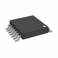
AD8367ARU-REEL7 Analog Devices Inc, AD8367ARU-REEL7 Datasheet - Page 11

AD8367ARU-REEL7
Manufacturer Part Number
AD8367ARU-REEL7
Description
IC,Voltage Controlled Gain Amplifier,SINGLE,TSSOP,14PIN,PLASTIC
Manufacturer
Analog Devices Inc
Series
X-AMP®r
Datasheet
1.AD8367-EVAL.pdf
(24 pages)
Specifications of AD8367ARU-REEL7
Rohs Status
RoHS non-compliant
Amplifier Type
Variable Gain
Number Of Circuits
1
-3db Bandwidth
500MHz
Current - Input Bias
27µA
Current - Supply
26mA
Voltage - Supply, Single/dual (±)
2.7 V ~ 5.5 V
Operating Temperature
-40°C ~ 85°C
Mounting Type
Surface Mount
Package / Case
14-TSSOP
Output Type
-
Current - Output / Channel
-
Slew Rate
-
Gain Bandwidth Product
-
Voltage - Input Offset
-
Lead Free Status / RoHS Status
THEORY OF OPERATION
The AD8367 is a variable gain, single-ended, IF amplifier based
on Analog Devices’ patented X-AMP architecture. It offers
accurate gain control with a 45 dB span and a 3 dB bandwidth
of 500 MHz. It can be configured as a traditional VGA with
50 dB/V gain scaling or as an AGC amplifier by using the built
in rms detector. Figure 27 is a simplified block diagram of the
amplifier. The main signal path consists of a voltage controlled
0 dB to 45 dB variable attenuator followed by a 42.5 dB fixed
gain amplifier. The AD8367 is designed to operate optimally in
a 200 Ω impedance system.
INPUT ATTENUATOR AND GAIN CONTROL
The variable attenuator consists of a 200 Ω single-ended
resistive ladder that comprises of nine 5 dB sections and an
interpolator that selects the attenuation factor. Each tap point
down the ladder network further attenuates the input signal
by a fixed decibel factor. Gain control is achieved by sensing
different tap points with variable transconductance stages.
Based on the gain control voltage, an interpolator selects which
stage(s) are active. For example, if only the first stage is active,
the 0 dB tap point is sensed; if the last stage is active, the 45 dB
tap point is sensed. Attenuation levels that fall between tap
points are achieved by having neighboring g
simultaneously, creating a weighted average of the discrete
tap point attenuations. In this way, a smooth, monotonic
attenuation function is synthesized, that is, linear-in-dB
with a very precise scaling.
The gain of the AD8367 can be an increasing or decreasing
function of the control voltage, V
the MODE pin is pulled up to the positive supply or down to
ground. When the MODE pin is high, the gain increases with
V
transfer function is given by
where V
Equation 1 contains the gain scaling factor of 50 dB/V (20
mV/dB) and the gain intercept of −5 dB, which represents the
extrapolated gain for V
to +42.5 dB for V
GAIN
GAIN
INPT
Gain (dB) = 50 × V
, as shown in Figure 28. The ideal linear-in-dB scaled
GAIN
g
m
GAIN INTERPOLATOR
200Ω
is expressed in volts.
0dB –5dB –10dB
ATTENUATOR LADDER
g
m
GAIN
Figure 27. Simplified Architecture
g
m
ranging from 50 mV to 950 mV. The
GAIN
GAIN
= 0 V. The gain ranges from −2.5 dB
− 5
g
m
–45dB
GAIN
, depending on whether
INTEGRATOR
V
OUT
–42.5dB
m
stages active
OUTPUT
BUFFER
VOUT
Rev. A | Page 11 of 24
(1)
deviation from Equation 1, that is, the gain conformance error,
is also illustrated in Figure 28. The ripples in the error are a
result of the interpolation action between
tap points. The AD8367 provides better than ±0.5 dB of
conformance error over >40 dB gain range at 200 MHz
and ±1 dB at 400 MHz.
The gain is a decreasing function of V
is low. Figure 28 also illustrates this mode, which is described by
This gain mode is required in AGC applications using the built-
in, square-law level detector.
INPUT AND OUTPUT INTERFACES
The AD8367 was designed to operate best in a 200 Ω imped-
ance system. Its gain range, conformance law, noise, and
distortion assume that 200 Ω source and load impedances
are used. Interfacing the AD8367 to other common impedances
(from 50 Ω used at radio frequencies to 1 kΩ presented by data
converters) can be accomplished using resistive or reactive
passive networks, whose design depends on specific system
requirements, such as bandwidth, return loss, noise figure,
and absolute gain range.
The input impedance of the AD8367 is nominally 200 Ω,
determined by the resistive ladder network. This presents a
200 Ω dc resistance to ground, and, in cases where an elevated
signal potential is used, ac coupling is necessary. The input
signal level must not exceed 700 mV p-p to avoid overloading
the input stage. The output impedance is determined by an
internal 50 Ω damping resistor, as shown in Figure 29. Despite
the fact that the output impedance is 50 Ω, the AD8367 should
still be presented with a load of 200 Ω. This implies that the
load is mismatched, but doing so preserves the distortion
performance of the amplifier.
Figure 28. The gain function can be either an increasing or decreasing
Gain (dB) = 45 − 50 × V
44
40
36
32
28
24
20
16
12
–4
8
4
0
0
0.1
function of V
0.2
HI MODE
LO MODE
0.3
GAIN
0.4
, depending on the MODE pin.
V
GAIN
GAIN
0.5
(V)
50dB/V
SLOPE
GAIN
0.6
GAIN
0.7
when the MODE pin
0.8
0.9
AD8367
1.0
2.0
1.6
1.2
0.8
0.4
0
–0.4
–0.8
–1.2
–1.6
–2.0
–2.4
(2)


