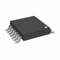
AD8367ARU-REEL7 Analog Devices Inc, AD8367ARU-REEL7 Datasheet - Page 17

AD8367ARU-REEL7
Manufacturer Part Number
AD8367ARU-REEL7
Description
IC,Voltage Controlled Gain Amplifier,SINGLE,TSSOP,14PIN,PLASTIC
Manufacturer
Analog Devices Inc
Series
X-AMP®r
Datasheet
1.AD8367-EVAL.pdf
(24 pages)
Specifications of AD8367ARU-REEL7
Rohs Status
RoHS non-compliant
Amplifier Type
Variable Gain
Number Of Circuits
1
-3db Bandwidth
500MHz
Current - Input Bias
27µA
Current - Supply
26mA
Voltage - Supply, Single/dual (±)
2.7 V ~ 5.5 V
Operating Temperature
-40°C ~ 85°C
Mounting Type
Surface Mount
Package / Case
14-TSSOP
Output Type
-
Current - Output / Channel
-
Slew Rate
-
Gain Bandwidth Product
-
Voltage - Input Offset
-
Lead Free Status / RoHS Status
Note that in this circuit the AD8367’s MODE pin must be
pulled high to obtain correct feedback polarity because the
integrator inverts the polarity of the feedback signal.
The relationship between the setpoint voltage and the rms
output voltage of the AD8367 is
where 225 is the input resistance of the AD8361 and 7.5 is its
conversion gain. For R1 = 200 Ω, this reduces to V
× 0.25.
Capacitor C2 sets the averaging time for the rms detector. This
should be made long enough to provide sufficient smoothing of
the detector’s output in the presence of the modulation on the
RF signal. A level fluctuation of less than 1 dB (<5% to 10%) p-p
at the AD8361’s output is a reasonable value. A considerably
longer time constant needlessly lowers the AGC bandwidth,
while a short time constant can degrade the accuracy of the
true-rms measurement process. Components C1, R2, and R3
set the control loop’s bandwidth and stability. The maximum
stable loop bandwidth is limited by the rms detector’s averaging
time constant as previously discussed.
For an input signal consisting of a 4.096 MS/s QPSK modulated
carrier, the relationship between V
this setup is shown in Figure 39. The exponential shape reflects
the linear-in-magnitude response of the AD8361. The adjacent
channel power ratio (ACPR) as a function of output power is
illustrated in Figure 40. The minima occur where the distortion
and integrated noise powers cross over.
V
OUT
−
RMS
=
V
INPUT
SET
×
J1
(
225
R1
57.6Ω
+
R6
×
225
V
7.5
10kΩ
g
10nF
R5
)
SET
and the output power for
Figure 38. Example of Using an External Detector to Form an AGC Loop
1
2
3
4
5
6
7
ICOM
ENBL
INPT
MODE
GAIN
DETO
ICOM
AD8367
U1
OUT –RMS
33kΩ
OCOM
VPSO
VOUT
R4
DECL
ICOM
HPFL
VPSI
= V
14
13
12
11
10
9
8
Rev. A | Page 17 of 24
V
(6)
AGC
SET
10nF
C
C5
10nF
HP
100Ω
R
HP
6
0.1μF
The component values shown in Figure 38 were chosen for a
64-QAM signal at 500 kS/s at a carrier frequency of 150 MHz.
The response time of the loop as shown is roughly 5 ms for
an abrupt input level change of 40 dB. Figure 41 shows the
dynamic performance of the loop with a step-modulated
CW signal applied to the input for a V
For a linear-in-dB response, detectors such as the AD8318 or
the AD8362 can be used in place of the AD8361.
AD820
0.1μF
3.3nF
5V
C1
2.2Ω
U3
4
7
4.0
3.5
3.0
2.5
2.0
1.5
1.0
0.5
0
–20
2
3
Figure 39. AGC Setpoint Voltage vs. Output Power
200kΩ
10nF
10nF
R3
82kΩ
R1
V
SET
–15
(QPSK: 4.096 MS/s; α = 0.22; 1 User)
1
2
3
4
20pF
VPOS
IREF
RFIN
PWDN
5V
V
200Ω LOAD
OUT
–10
AD8361
POUT (dBm INTO 200Ω)
INTO A
U2
150kΩ
COMM
R2
VRMS
SREF
FLTR
–5
0.27μF
C2
8
7
6
5
12kΩ
SET
10MHz
of about 1 V.
0
Vrms
380MHz
5
AD8367
10


