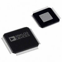
AD9773BSVRL Analog Devices Inc, AD9773BSVRL Datasheet - Page 18

AD9773BSVRL
Manufacturer Part Number
AD9773BSVRL
Description
IC,D/A CONVERTER,DUAL,12-BIT,CMOS,TQFP,80PIN
Manufacturer
Analog Devices Inc
Series
TxDAC®r
Datasheet
1.AD9773BSVZRL.pdf
(60 pages)
Specifications of AD9773BSVRL
Rohs Status
RoHS non-compliant
Settling Time
11ns
Number Of Bits
12
Data Interface
Serial, SPI™
Number Of Converters
2
Voltage Supply Source
Analog and Digital
Power Dissipation (max)
410mW
Operating Temperature
-40°C ~ 85°C
Mounting Type
Surface Mount
Package / Case
80-TQFP Exposed Pad, 80-eTQFP, 80-HTQFP, 80-VQFP
For Use With
AD9773-EBZ - BOARD EVALUATION AD9773
Lead Free Status / RoHS Status
AD9773
MODE CONTROL (VIA SPI PORT)
Table 9. Mode Control via SPI Port
Address
00h
01h
02h
03h
04h
05h
06h
07h
08h
09h
Bit 7
SDIO
Bidirectional
0 = Input
1 = I/O
Filter
Interpolation
Rate
(1×, 2×, 4×, 8×)
0 = Signed
Input Data
1 = Unsigned
Data Rate
Output Clock
0 = PLL OFF
1 = PLL ON
IDAC
Fine Gain
Adjustment
IDAC Offset
Adjustment
Bit 9
IDAC I
Direction
0 = I
on I
1 = I
on I
QDAC
Fine Gain
Adjustment
OUTB
OUTA
OFFSET
OFFSET
OFFSET
2
2
Bit 6
LSB, MSB First
0 = MSB
1 = LSB
Filter
Interpolation
Rate
(1×, 2×, 4×, 8×)
0 = Two-Port
Mode
1 = One-Port
Mode
0 = Automatic
Charge Pump
Control
1 =
Programmable
IDAC
Fine Gain
Adjustment
IDAC Offset
Adjustment
Bit 8
QDAC
Fine Gain
Adjustment
1
Bit 5
Software
Reset
on Logic 1
Modulation
Mode
(None, f
f
DATACLK
Driver
Strength
IDAC
Fine Gain
Adjustment
IDAC Offset
Adjustment
Bit 7
QDAC
Fine Gain
Adjustment
S
/4, f
S
/8)
S
/2,
Rev. D | Page 18 of 60
Bit 4
Sleep
Mode
Logic 1
Shuts
Down the
DAC
Output
Currents
Modulation
Mode
(None, f
f
DATACLK
Invert
0 = No
Invert
1 = Invert
IDAC
Fine Gain
Adjustment
IDAC Offset
Adjustment
Bit 6
QDAC
Fine Gain
Adjustment
S
/4, f
S
/8)
S
/2,
Bit 3
Power-Down
Mode Logic 1
Shuts Down
All Digital and
Analog
Functions
0 = No Zero
Stuffing on
Interpolation
Filters, Logic 1
Enables Zero
Stuffing
IDAC
Fine Gain
Adjustment
IDAC
Coarse Gain
Adjustment
IDAC Offset
Adjustment
Bit 5
QDAC
Fine Gain
Adjustment
Bit 2
1R/2R Mode
DAC Output
Current Set by
One or Two
External
Resistors
0 = 2R, 1 = 1R
1 = Real Mix
Mode
0 = Complex
Mix Mode
ONEPORTCLK
Invert
0 = No Invert
1 = Invert
PLL Charge
Pump
Control
IDAC
Fine Gain
Adjustment
IDAC
Coarse Gain
Adjustment
IDAC Offset
Adjustment
Bit 4
QDAC
Fine Gain
Adjustment
Bit 1
PLL_LOCK
Indicator
0 = e
1 = e
IQSEL
Invert
0 = No
Invert
1 = Invert
PLL Divide
(Prescaler)
Ratio
PLL Charge
Pump
Control
IDAC
Fine Gain
Adjustment
IDAC
Coarse
Gain
Adjustment
IDAC Offset
Adjustment
Bit 3
IDAC Offset
Adjustment
Bit 1
QDAC
Fine Gain
Adjustment
+jωt
–jωt
Bit 0
DATACLK/
PLL_LOCK
Select
0 =
PLLLOCK
1 =
DATACLK
Q First
0 = I First
1 = Q First
PLL Divide
(Prescaler)
Ratio
PLL Charge
Pump
Control
IDAC
Fine Gain
Adjustment
IDAC
Coarse
Gain
Adjustment
IDAC Offset
Adjustment
Bit 2
IDAC Offset
Adjustment
Bit 0
QDAC
Fine Gain
Adjustment
2


