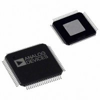
AD9773BSVRL Analog Devices Inc, AD9773BSVRL Datasheet - Page 5

AD9773BSVRL
Manufacturer Part Number
AD9773BSVRL
Description
IC,D/A CONVERTER,DUAL,12-BIT,CMOS,TQFP,80PIN
Manufacturer
Analog Devices Inc
Series
TxDAC®r
Datasheet
1.AD9773BSVZRL.pdf
(60 pages)
Specifications of AD9773BSVRL
Rohs Status
RoHS non-compliant
Settling Time
11ns
Number Of Bits
12
Data Interface
Serial, SPI™
Number Of Converters
2
Voltage Supply Source
Analog and Digital
Power Dissipation (max)
410mW
Operating Temperature
-40°C ~ 85°C
Mounting Type
Surface Mount
Package / Case
80-TQFP Exposed Pad, 80-eTQFP, 80-HTQFP, 80-VQFP
For Use With
AD9773-EBZ - BOARD EVALUATION AD9773
Lead Free Status / RoHS Status
SPECIFICATIONS
DC SPECIFICATIONS
T
Table 1.
Parameter
RESOLUTION
ANALOG OUTPUT (for IR and 2R Gain Setting Modes)
REFERENCE OUTPUT
REFERENCE INPUT
TEMPERATURE COEFFICIENTS
POWER SUPPLY
OPERATING RANGE
1
2
3
4
5
Measured at I
Nominal full-scale current, I
Use an external amplifier to drive any external load.
100 MSPS f
400 MSPS f
MIN
DC Accuracy
Offset Error
Gain Error (with Internal Reference)
Gain Matching
Full-Scale Output Current
Output Compliance Range
Output Resistance
Output Capacitance
Gain, Offset Cal DACs, Monotonicity Guaranteed
Reference Voltage
Reference Output Current
Input Compliance Range
Reference Input Resistance
Small Signal Bandwidth
Offset Drift
Gain Drift (With Internal Reference)
Reference Voltage Drift
AVDD
CLKVDD
CLKVDD (PLL ON)
DVDD
P
P
Power Supply Rejection Ratio—AVDD
DIS
DIS
Integral Nonlinearity
Differential Nonlinearity
Monotonicity
Voltage Range
Analog Supply Current (I
I
Voltage Range
Clock Supply Current (I
Clock Supply Current (I
Voltage Range
Digital Supply Current (I
Nominal Power Dissipation
to T
AVDD
5
in PWDN
MAX
in Sleep Mode
DAC
DAC
OUTA
, f
, AVDD = 3.3 V, CLKVDD = 3.3 V, DVDD = 3.3 V, PLLVDD = 3.3 V, I
with f
DATA
1
driving a virtual ground.
= 50 MSPS, f
OUT
= 1 MHz, all supplies = 3.3 V, no interpolation, no modulation.
OUTFS
, is 32× the I
S
CLKVDD
CLKVDD
2
/2 modulation, PLL enabled.
3
DVDD
AVDD
)
)
)
)
4
4
4
REF
current.
Rev. D | Page 5 of 60
Min
12
−1.5
−1
−0.02
−1.0
−1.0
2
−1.0
1.14
0.1
3.1
3.1
3.1
−40
OUTFS
Guaranteed over specified temperature range
Typ
±0.4
±0.2
±0.01
200
3
1.20
100
7
0.5
±50
3.3
72.5
3.3
8.5
23.5
3.3
34
1.75
6.0
±0.4
±0.1
0
50
23.3
380
= 20 mA, unless otherwise noted.
Max
+1.5
+1
+0.02
+1.0
+1.0
20
+1.25
1.26
1.25
3.5
76
26
3.5
10.0
3.5
41
410
+85
Unit
Bits
LSB
LSB
% of FSR
% of FSR
% of FSR
mA
V
kΩ
pF
V
nA
V
kΩ
MHz
ppm of FSR/°C
ppm of FSR/°C
ppm/°C
V
mA
mA
V
mA
mA
V
mA
mW
W
mW
% of FSR/V
°C
AD9773


