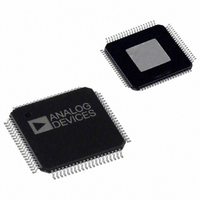
AD9773BSVRL Analog Devices Inc, AD9773BSVRL Datasheet - Page 26

AD9773BSVRL
Manufacturer Part Number
AD9773BSVRL
Description
IC,D/A CONVERTER,DUAL,12-BIT,CMOS,TQFP,80PIN
Manufacturer
Analog Devices Inc
Series
TxDAC®r
Datasheet
1.AD9773BSVZRL.pdf
(60 pages)
Specifications of AD9773BSVRL
Rohs Status
RoHS non-compliant
Settling Time
11ns
Number Of Bits
12
Data Interface
Serial, SPI™
Number Of Converters
2
Voltage Supply Source
Analog and Digital
Power Dissipation (max)
410mW
Operating Temperature
-40°C ~ 85°C
Mounting Type
Surface Mount
Package / Case
80-TQFP Exposed Pad, 80-eTQFP, 80-HTQFP, 80-VQFP
For Use With
AD9773-EBZ - BOARD EVALUATION AD9773
Lead Free Status / RoHS Status
AD9773
The offset control defines a small current that can be added
to I
selection in which I
is programmable via Register 08h, Bit 7 (IDAC) and Register
0Ch, Bit 7 (QDAC). Figure 41 shows the scale of the offset
current that can be added to one of the complementary outputs
on the IDAC and QDAC. Offset control can be used for
suppression of LO leakage resulting from modulation of dc
signal components. If the AD9773 is dc-coupled to an external
modulator, this feature can be used to cancel the output offset
on the AD9773 as well as the input offset on the modulator.
Figure 42 shows a typical example of the effect that the offset
control has on LO suppression.
In Figure 42, the negative scale represents an offset added to
I
of the respective DAC. Offset Register 1 corresponds to IDAC,
while Offset Register 2 corresponds to QDAC. Figure 42
represents the AD9773 synthesizing a complex signal that is
then dc-coupled to an AD8345 quadrature modulator with an
LO of 800 MHz. The dc coupling allows the input offset of the
AD8345 to be calibrated out as well. The LO suppression at the
AD8345 output was optimized first by adjusting Offset Register 1
in the AD9773. When an optimal point was found (roughly
Code 54), this code was held in Offset Register 1, and Offset
Register 2 was adjusted. The resulting LO suppression is
70 dBFS. These are typical numbers, and the specific code for
optimization varies from part to part.
OUTB
OUTA
–0.5
–1.0
–1.5
–2.0
–2.5
–3.0
, while the positive scale represents an offset added to I
0
0
or I
OUTB
(not both) on the IDAC and QDAC. The
200
Figure 40. Fine Gain Effect on I
(ASSUMING R
OUT
FINE GAIN REGISTER CODE
for this offset current is directed toward
400
SET
1, R
SET
600
2 = 1.9k Ω )
1R MODE
2R MODE
FULLSCALE
800
1000
OUTA
Rev. D | Page 26 of 60
1R/2R MODE
In 2R mode, the reference current for each channel is set
independently by the FSADJ resistor on that channel. The
AD9773 can be programmed to derive its reference current
from a single resistor on Pin 60 by putting the part into 1R
mode. The transfer functions in Equation 1 are valid for 2R
mode. In 1R mode, the current developed in the single FSADJ
resistor is split equally between the two channels. The result is
that in 1R mode, a scale factor of 1/2 must be applied to the
formulas in Equation 1. The full-scale DAC current in 1R mode
can still be set to as high as 20 mA by using the internal 1.2 V
reference and a 950 Ω resistor instead of the 1.9 kΩ resistor
typically used in 2R mode.
–10
–20
–30
–40
–50
–60
–70
–80
–1024
0
5
4
3
2
1
0
0
0
Figure 42. Offset Adjust Control, Effect on LO Suppression
–768
200
DAC1, DAC2 (OFFSET REGISTER CODES)
Figure 41. DAC Output Offset Current
–512
(ASSUMING RSET1, RSET2 = 1.9k Ω )
COARSE GAIN REGISTER CODE
–256
400
OFFSET REGISTER 1 ADJUSTED
0
600
OFFSET REGISTER 2
ADJUSTED, WITH OFFSET
REGISTER 1 SET
TO OPTIMIZED VALUE
256
2R MODE
512
800
1R MODE
768
1000
1024


