AD9779A-EBZ Analog Devices Inc, AD9779A-EBZ Datasheet - Page 40
AD9779A-EBZ
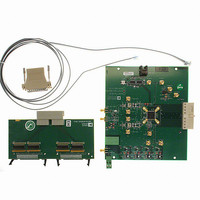
Manufacturer Part Number
AD9779A-EBZ
Description
Dual 16B, 1.0 GSPS TxDAC
Manufacturer
Analog Devices Inc
Series
TxDAC®r
Datasheet
1.AD9776ABSVZ.pdf
(60 pages)
Specifications of AD9779A-EBZ
Design Resources
Interfacing ADL5370 to AD9779A Dual-Channel, 1 GSPS High Speed DAC (CN0016) Interfacing ADL5371 to AD9779A Dual-Channel, 1 GSPS High Speed DAC (CN0017) Interfacing ADL5372 to AD9779A Dual-Channel, 1 GSPS High Speed DAC (CN0018) Interfacing ADL5373 to AD9779A Dual-Channel, 1 GSPS High Speed DAC (CN0019) Interfacing ADL5374 to AD9779A Dual-Channel, 1 GSPS High Speed DAC (CN0020) Interfacing ADL5375 to AD9779A Dual-Channel, 1 GSPS High Speed DAC (CN0021)
Number Of Dac's
2
Number Of Bits
16
Outputs And Type
2, Differential
Sampling Rate (per Second)
1G
Data Interface
Serial
Dac Type
Current
Voltage Supply Source
Analog and Digital
Operating Temperature
-40°C ~ 85°C
Utilized Ic / Part
AD9779A
Lead Free Status / RoHS Status
Lead free / RoHS Compliant
Settling Time
-
Lead Free Status / RoHS Status
Lead free / RoHS Compliant


AD9776A/AD9778A/AD9779A
TRANSMIT PATH GAIN AND OFFSET CORRECTION
Analog quadrature modulators make it very easy to realize
single sideband radios. However, there are several nonideal
aspects of quadrature modulator performance. Among these
analog degradations are
•
•
The AD9776A/AD9778A/AD9779A have the capability to
correct for both of these analog degradations. Note that these
degradations drift over temperature; therefore, if close to optimal
single sideband performance is desired, a scheme for sensing
these degradations over temperature and correcting for them
may be necessary.
I/Q CHANNEL GAIN MATCHING
Gain matching is achieved by adjusting the values in the DAC
gain registers. For the I DAC, these values are in the I DAC
Control Register 0x05. For the Q DAC, these values are in the
Q DAC Control Register 0x07. These are 10-bit values. To
perform gain compensation, raise or lower the value of one of
these registers by a fixed step size and measure the amplitude
of the unwanted image. If the unwanted image is increasing in
amplitude, stop the procedure and try the same adjustment on
the other DAC control register. Do this until the image rejection
cannot be improved through further adjustment of these registers.
It should be noted that LO feedthrough compensation is inde-
pendent of phase compensation. However, gain compensation
could affect the LO compensation because the gain compensa-
tion may change the common-mode level of the signal. The dc
offset of some modulators is common-mode level dependent.
Therefore, it is recommended that the gain adjustment is
performed prior to LO compensation.
AUXILIARY DAC OPERATION
Two auxiliary DACs are provided on the AD9776A/AD9778A/
AD9779A. The full-scale output current on these DACs is derived
from the 1.2 V band gap reference and external resistor between
the I120 pin and ground. The gain scale from the reference
amplifier current (I
current is 16.67 with the auxiliary DAC gain set to full scale
(10-bit values, SPI Register 0x0D and SPI Register 0x11), this
Gain mismatch—the gain in the real and imaginary signal
paths of the quadrature modulator may not be matched
perfectly. This leads to less than optimal image rejection as
the cancellation of the negative frequency image is less than
perfect.
LO feedthrough—the quadrature modulator has a finite dc
referred offset, as well as coupling from its LO port to the
signal inputs. These can lead to a significant spectral spurs
at the frequency of the quadrature modulator LO.
REFERENCE
) to the auxiliary DAC reference
Rev. A | Page 40 of 60
gives a full-scale current of approximately 2 mA for AUX DAC1
and AUX DAC2.
The AUX DAC structure is shown in Figure 77. Only one of
the two output pins of the AUX DAC is active at a time. The
inactive side goes to a high impedance state (>100 kΩ). The
active output pin is chosen by writing to Register 0x0E and
Register 0x10, Bit 7.
The active output can act as either a current source or a current
sink. When sourcing current, the output compliance voltage is
0 V to 1.6 V. When sinking current, the output compliance voltage
is 0.8 V to 1.6 V. The output pin is chosen to be a current source
or current sink by writing to Register 0x0E and Register 0x10, Bit 6.
The magnitude of the AUX DAC1 current is controlled by the
AUX DAC1 Control Register 0x0D, and the magnitude of the
AUX DAC2 current is controlled by the AUX DAC2 Control
Register 0x11. These AUX DACs have the ability to source or
sink current. This is programmable via Bit 14 in either AUX
DAC control register. The choice of sinking or sourcing should
be made at circuit design time. There is no advantage to switch-
ing between source or sinking current once the circuit is in place.
The auxiliary DACs can be used for local oscillator (LO)
cancellation when the DAC output is followed by a quadrature
modulator. This LO feedthrough is caused by the input referred
dc offset voltage of the quadrature modulator (and the DAC
output offset voltage mismatch) and can degrade system perform-
ance. Typical DAC-to-quadrature modulator interfaces are
shown in Figure 78 and Figure 79. Often, the input common-
mode voltage for the modulator is much higher than the output
compliance range of the DAC, so that ac coupling or a dc level
shift is necessary. If the required common-mode input voltage
on the quadrature modulator matches that of the DAC, then the
dc blocking capacitors in Figure 78 can be removed. A low-pass
or band-pass passive filter is recommended when spurious signals
from the DAC (distortion and DAC images) at the quadrature
modulator inputs can affect the system performance. Placing the
filter at the location shown in Figure 78 and Figure 79 allows
easy design of the filter, as the source and load impedances can
easily be designed close to 50 Ω.
Figure 77. Auxiliary DAC Structure on AD9776A/AD9778A/AD97779A
(SOURCE)
0 TO 2mA
0 TO 2mA
(SINK)
V
BIAS
SOURCE/
SINC
P/N
AUXP
AUXN
Related parts for AD9779A-EBZ
Image
Part Number
Description
Manufacturer
Datasheet
Request
R

Part Number:
Description:
Dual 16B, 1.0 GSPS TxDAC
Manufacturer:
Analog Devices Inc
Datasheet:
Part Number:
Description:
BOARD EVALUATION FOR AD9779
Manufacturer:
Analog Devices Inc
Datasheet:
Part Number:
Description:
BOARD EVALUATION FOR AD9779
Manufacturer:
Analog Devices Inc
Datasheet:

Part Number:
Description:
±1.7g Dual-Axis IMEMS Accelerometer Evaluation Board
Manufacturer:
Analog Devices Inc
Datasheet:
Part Number:
Description:
Inertial Sensor Evaluation System
Manufacturer:
Analog Devices Inc
Datasheet:
Part Number:
Description:
Manufacturer:
Analog Devices Inc
Datasheet:
Part Number:
Description:
Manufacturer:
Analog Devices Inc
Datasheet:
Part Number:
Description:
Manufacturer:
Analog Devices Inc
Datasheet:
Part Number:
Description:
Manufacturer:
Analog Devices Inc
Datasheet:
Part Number:
Description:
Manufacturer:
Analog Devices Inc
Datasheet:
Part Number:
Description:
Manufacturer:
Analog Devices Inc
Datasheet:
Part Number:
Description:
Manufacturer:
Analog Devices Inc
Datasheet:
Part Number:
Description:
Manufacturer:
Analog Devices Inc
Datasheet: