AD9779A-EBZ Analog Devices Inc, AD9779A-EBZ Datasheet - Page 5
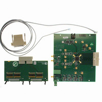
AD9779A-EBZ
Manufacturer Part Number
AD9779A-EBZ
Description
Dual 16B, 1.0 GSPS TxDAC
Manufacturer
Analog Devices Inc
Series
TxDAC®r
Datasheet
1.AD9776ABSVZ.pdf
(60 pages)
Specifications of AD9779A-EBZ
Design Resources
Interfacing ADL5370 to AD9779A Dual-Channel, 1 GSPS High Speed DAC (CN0016) Interfacing ADL5371 to AD9779A Dual-Channel, 1 GSPS High Speed DAC (CN0017) Interfacing ADL5372 to AD9779A Dual-Channel, 1 GSPS High Speed DAC (CN0018) Interfacing ADL5373 to AD9779A Dual-Channel, 1 GSPS High Speed DAC (CN0019) Interfacing ADL5374 to AD9779A Dual-Channel, 1 GSPS High Speed DAC (CN0020) Interfacing ADL5375 to AD9779A Dual-Channel, 1 GSPS High Speed DAC (CN0021)
Number Of Dac's
2
Number Of Bits
16
Outputs And Type
2, Differential
Sampling Rate (per Second)
1G
Data Interface
Serial
Dac Type
Current
Voltage Supply Source
Analog and Digital
Operating Temperature
-40°C ~ 85°C
Utilized Ic / Part
AD9779A
Lead Free Status / RoHS Status
Lead free / RoHS Compliant
Settling Time
-
Lead Free Status / RoHS Status
Lead free / RoHS Compliant


DIGITAL SPECIFICATIONS
T
otherwise noted. LVDS driver and receiver are compliant to the IEEE-1596 reduced range link, unless otherwise noted.
Table 2.
Parameter
CMOS INPUT LOGIC LEVEL
CMOS OUTPUT LOGIC LEVEL (DATACLK, PIN 37)
LVDS RECEIVER INPUTS (SYNC_I+, SYNC_I−)
LVDS DRIVER OUTPUTS (SYNC_O+, SYNC_O−)
DAC CLOCK INPUT (REFCLK+, REFCLK−)
SERIAL PERIPHERAL INTERFACE
1
Specification is at a DATACLK frequency of 100 MHz into a 1 kΩ load, maximum drive capability of 8 mA. At higher speeds or greater loads, best practice suggests
using an external buffer for this signal.
MIN
Input V
Input V
Maximum Input Data Rate at Interpolation
Output V
Output V
DATACLK Output Duty Cycle
Input Voltage Range, V
Input Differential Threshold, V
Input Differential Hysteresis, V
Receiver Differential Input Impedance, R
LVDS Input Rate
Setup Time, SYNC_I to REFCLK
Hold Time, SYNC_I to REFCLK
Output Voltage High, V
Output Voltage Low, V
Output Differential Voltage, |V
Output Offset Voltage, V
Output Impedance, R
Differential Peak-to-Peak Voltage
Common-Mode Voltage
Maximum Clock Rate
Maximum Clock Rate (SCLK)
Minimum Pulse Width High
Minimum Pulse Width Low
Setup Time, SDI to SCLK
Hold Time, SDI to SCLK
Data Valid, SDO to SCLK
to T
1×
2×
4×
8×
MAX
IN
IN
Logic High
Logic Low
OUT
OUT
, AVDD33 = 3.3 V, DVDD33 = 3.3 V, DVDD18 = 1.8 V, CVDD18 = 1.8 V, I
Logic High
Logic Low
O
OA
IA
OA
OS
or V
or V
or V
IB
OB
OB
IDTH
IDTHH
OD
|
− V
IDTHL
IN
1
Conditions
DVDD18, CVDD18 = 1.9 V ± 5%
DVDD18, CVDD18 = 2.0 V ± 2%
At 250 MHz, into 5 pF load
SYNC_I+ = V
Additional limits on f
Register 5, Bits<3:1> in Table 14
SYNC_O+ = V
Single-ended
DVDD18, CVDD18 = 1.9 V ± 5%
DVDD18, CVDD18 = 2.0 V ± 2%
DVDD18, CVDD18 = 1.8 V ± 5%
DVDD18, CVDD18 = 1.8 V ± 5%
Rev. A | Page 5 of 60
IA
OA
, SYNC_I− = V
, SYNC_O− = V
SYNC_I
apply; see description of
IB
OB
, 100 Ω termination
OUTFs
= 20 mA, maximum sample rate, unless
AD9776A/AD9778A/AD9779A
Min
2.0
300
250
200
112.5
125
137.5
2.4
40
825
−100
80
0.4
0.55
1025
150
1150
80
400
300
900
1000
1100
40
1.6
0.0
2.0
Typ
50
20
200
100
800
400
Max
0.8
0.4
60
1575
+100
120
250
1375
250
1250
120
2000
500
12.5
12.5
Unit
V
V
MSPS
MSPS
MSPS
MSPS
MSPS
MSPS
V
V
%
mV
mV
mV
Ω
MSPS
ns
ns
mV
mV
mV
mV
Ω
mV
mV
MSPS
MSPS
MSPS
MHz
ns
ns
ns
ns
ns
Related parts for AD9779A-EBZ
Image
Part Number
Description
Manufacturer
Datasheet
Request
R

Part Number:
Description:
Dual 16B, 1.0 GSPS TxDAC
Manufacturer:
Analog Devices Inc
Datasheet:
Part Number:
Description:
BOARD EVALUATION FOR AD9779
Manufacturer:
Analog Devices Inc
Datasheet:
Part Number:
Description:
BOARD EVALUATION FOR AD9779
Manufacturer:
Analog Devices Inc
Datasheet:

Part Number:
Description:
±1.7g Dual-Axis IMEMS Accelerometer Evaluation Board
Manufacturer:
Analog Devices Inc
Datasheet:
Part Number:
Description:
Inertial Sensor Evaluation System
Manufacturer:
Analog Devices Inc
Datasheet:
Part Number:
Description:
Manufacturer:
Analog Devices Inc
Datasheet:
Part Number:
Description:
Manufacturer:
Analog Devices Inc
Datasheet:
Part Number:
Description:
Manufacturer:
Analog Devices Inc
Datasheet:
Part Number:
Description:
Manufacturer:
Analog Devices Inc
Datasheet:
Part Number:
Description:
Manufacturer:
Analog Devices Inc
Datasheet:
Part Number:
Description:
Manufacturer:
Analog Devices Inc
Datasheet:
Part Number:
Description:
Manufacturer:
Analog Devices Inc
Datasheet:
Part Number:
Description:
Manufacturer:
Analog Devices Inc
Datasheet: