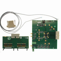
AD9779A-EBZ Analog Devices Inc, AD9779A-EBZ Datasheet - Page 48

AD9779A-EBZ
Manufacturer Part Number
AD9779A-EBZ
Description
Dual 16B, 1.0 GSPS TxDAC
Manufacturer
Analog Devices Inc
Series
TxDAC®r
Datasheet
1.AD9776ABSVZ.pdf
(60 pages)
Specifications of AD9779A-EBZ
Design Resources
Interfacing ADL5370 to AD9779A Dual-Channel, 1 GSPS High Speed DAC (CN0016) Interfacing ADL5371 to AD9779A Dual-Channel, 1 GSPS High Speed DAC (CN0017) Interfacing ADL5372 to AD9779A Dual-Channel, 1 GSPS High Speed DAC (CN0018) Interfacing ADL5373 to AD9779A Dual-Channel, 1 GSPS High Speed DAC (CN0019) Interfacing ADL5374 to AD9779A Dual-Channel, 1 GSPS High Speed DAC (CN0020) Interfacing ADL5375 to AD9779A Dual-Channel, 1 GSPS High Speed DAC (CN0021)
Number Of Dac's
2
Number Of Bits
16
Outputs And Type
2, Differential
Sampling Rate (per Second)
1G
Data Interface
Serial
Dac Type
Current
Voltage Supply Source
Analog and Digital
Operating Temperature
-40°C ~ 85°C
Utilized Ic / Part
AD9779A
Lead Free Status / RoHS Status
Lead free / RoHS Compliant
Settling Time
-
Lead Free Status / RoHS Status
Lead free / RoHS Compliant
AD9776A/AD9778A/AD9779A
Figure 97. Power Dissipation, Clock 1.8 V Supply, I and Q Data, Dual DAC
0.075
0.050
0.025
0.125
0.100
0.075
0.050
0.025
0.16
0.14
0.12
0.10
0.08
0.06
0.04
0.02
Figure 98. Power Dissipation, Digital 3.3 V Supply, I and Q Data,
0
Figure 99. DVDD18 Power Dissipation of Inverse Sinc Filter
0
0
0
0
0
8× INTERPOLATION, f
ALL INTERPOLATION MODES
25
25
200
Mode, Does Not Include Zero Stuffing
NO MODULATION
50
50
75
75
400
Dual DAC Mode
f
f
DAC
DAC
DAC
100
100
f
f
f
DATA
DATA
DAC
/8,
/4,
/2,
600
125
125
(MSPS)
(MSPS)
(MSPS)
4× INTERPOLATION
150
150
1× INTERPOLATION,
800
NO MODULATION
2× INTERPOLATION
175
175
200
200
1000
225
225
1200
250
250
Rev. A | Page 48 of 60
POWER-DOWN AND SLEEP MODES
The AD9776A/AD9778A/AD9779A have a variety of power-
down modes; thus, the digital engine, main TxDACs, or auxiliary
DACs can be powered down individually or together. Via the SPI
port, the main TxDACs can be placed in sleep or power-down
mode. In sleep mode, the TxDAC output is turned off, thus
reducing power dissipation. The reference remains powered on,
however, so that recovery from sleep mode is very fast. With the
power-down mode bit set (Register 0x00, Bit 4), all analog and
digital circuitry, including the reference, is powered down. The
SPI port remains active in this mode. This mode offers more
substantial power savings than sleep mode, but the turn-on
time is much longer. The auxiliary DACs also have the capability
to be programmed into sleep mode via the SPI port. The Auto
Power-Down Enable bit (Register 0x00, Bit 3) controls the
power-down function for the digital section of the devices. The
auto power-down function works in conjunction with the
TXENABLE pin (Pin 39) according to Table 28.
Table 28.
TXENABLE
(Pin 39)
0
1
As shown in Figure 100, the power dissipation saved by using
the power-down mode is nearly proportional to the duty cycle
of the signal at the TXENABLE pin.
(If the TxEnable Invert bit (Register 0x02, Bit 1) is set, the function of the
0.9
0.8
0.7
0.6
0.5
0.4
0.3
0.2
0.1
Figure 100. Power Savings Based on Duty Cycle of TXENABLE
0
0
Description
If Auto Power-Down Enable bit = 0, flush data
path with 0s.
If Auto Power-Down Enable bit = 1, flush data
for multiple REFCLK cycles; then automatically
place the digital engine in power-down state.
DACs, reference, and SPI port are not affected.
Normal operation.
20
TXENABLE pin is inverted)
DUTY CYCLE (%)
40
60
2× INT
2× INT
4× INT
4× INT
8× INT
8× INT
f
f
f
f
f
f
DATA
DATA
DATA
DATA
DATA
DATA
80
= 50MSPS
= 200MSPS
= 50MSPS
= 200MSPS
= 50MSPS
= 200MSPS
1
00


