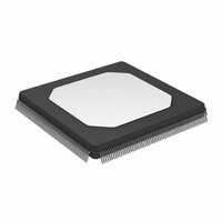
ADSP-21060KS-160 Analog Devices Inc, ADSP-21060KS-160 Datasheet - Page 10

ADSP-21060KS-160
Manufacturer Part Number
ADSP-21060KS-160
Description
Digital Signal Processor IC
Manufacturer
Analog Devices Inc
Series
SHARC®r
Type
Floating Pointr
Datasheets
1.ADSP-21062KSZ-133.pdf
(64 pages)
2.ADSP-21060KS-160.pdf
(47 pages)
3.ADSP-21060KS-160.pdf
(64 pages)
Specifications of ADSP-21060KS-160
Supply Voltage Max
5.25V
Dsp Type
Fixed / Floating Point
Mounting Type
Surface Mount
Package / Case
240-MQFP
Memory Organization - Ram
4M
Rohs Status
RoHS non-compliant
Interface
Host Interface, Link Port, Serial Port
Clock Rate
40MHz
Non-volatile Memory
External
On-chip Ram
512kB
Voltage - I/o
5.00V
Voltage - Core
5.00V
Operating Temperature
0°C ~ 85°C
Device Core Size
32b
Architecture
Super Harvard
Format
Floating Point
Clock Freq (max)
40MHz
Mips
40
Device Input Clock Speed
40MHz
Ram Size
512KB
Operating Supply Voltage (typ)
5V
Operating Supply Voltage (min)
4.75V
Operating Supply Voltage (max)
5.25V
Operating Temp Range
0C to 85C
Operating Temperature Classification
Commercial
Mounting
Surface Mount
Pin Count
240
Package Type
MQFP
Lead Free Status / Rohs Status
Not Compliant
Available stocks
Company
Part Number
Manufacturer
Quantity
Price
Company:
Part Number:
ADSP-21060KS-160
Manufacturer:
AD
Quantity:
5 510
Company:
Part Number:
ADSP-21060KS-160
Manufacturer:
SHARP
Quantity:
5 510
Company:
Part Number:
ADSP-21060KS-160
Manufacturer:
Analog Devices Inc
Quantity:
10 000
Pin
TFSx
RFSx
LxDAT
LxCLK
LxACK
EBOOT
LBOOT
BMS
CLKIN
RESET
TCK
TMS
TDI
TDO
TRST
EMU (O/D)
ICSA
VDD
GND
NC
ADSP-21060/ADSP-21060L
3-0
Type
I/O
I/O
I/O
I/O
I/O
I
I
I/O/T*
I
I/A
I
I/S
I/S
O
I/A
O
O
P
G
Function
Transmit Frame Sync (Serial Ports 0, 1).
Receive Frame Sync (Serial Ports 0, 1).
Link Port Data (Link Ports 0–5). Each LxCLK pin has a 50 kΩ internal pull-down resistor that is
enabled or disabled by the LPDRD bit of the LCOM register.
Link Port Clock (Link Ports 0–5). Each LxCLK pin has a 50 kΩ internal pull-down resistor that is
enabled or disabled by the LPDRD bit of the LCOM register.
Link Port Acknowledge (Link Ports 0–5). Each LxACK pin has a 50 kΩ internal pull-down resistor
that is enabled or disabled by the LPDRD bit of the LCOM register.
EPROM Boot Select. When EBOOT is high, the ADSP-2106x is configured for booting from an 8-
bit EPROM. When EBOOT is low, the LBOOT and BMS inputs determine booting mode. See table
below. This signal is a system configuration selection that should be hardwired.
Link Boot. When LBOOT is high, the ADSP-2106x is configured for link port booting. When
LBOOT is low, the ADSP-2106x is configured for host processor booting or no booting. See table
below. This signal is a system configuration selection that should be hardwired.
Boot Memory Select. Output: Used as chip select for boot EPROM devices (when EBOOT = 1,
LBOOT = 0). In a multiprocessor system, BMS is output by the bus master. Input: When low, indi-
cates that no booting will occur and that ADSP-2106x will begin executing instructions from external
memory. See table below. This input is a system configuration selection that should be hardwired.
*Three-statable only in EPROM boot mode (when BMS is an output).
EBOOT
1
0
0
0
0
1
Clock In. External clock input to the ADSP-2106x. The instruction cycle rate is equal to CLKIN.
CLKIN may not be halted, changed, or operated below the minimum specified frequency.
Processor Reset. Resets the ADSP-2106x to a known state and begins execution at the program
memory location specified by the hardware reset vector address. This input must be asserted (low) at
power-up.
Test Clock (JTAG). Provides an asynchronous clock for JTAG boundary scan.
Test Mode Select (JTAG). Used to control the test state machine. TMS has a 20 kΩ internal pull-up
resistor.
Test Data Input (JTAG). Provides serial data for the boundary scan logic. TDI has a 20 kΩ internal
pull-up resistor.
Test Data Output (JTAG). Serial scan output of the boundary scan path.
Test Reset (JTAG). Resets the test state machine. TRST must be asserted (pulsed low) after power-
up or held low for proper operation of the ADSP-2106x. TRST has a 20 kΩ internal pull-up resistor.
Emulation Status. Must be connected to the ADSP-2106x EZ-ICE target board connector only.
Reserved, leave unconnected.
Power Supply; nominally +5.0 V dc for 5 V devices or +3.3 V dc for 3.3 V devices. (30 pins).
Power Supply Return. (30 pins).
Do Not Connect. Reserved pins which must be left open and unconnected.
LBOOT
0
0
1
0
1
1
BMS
Output
1 (Input)
1 (Input)
0 (Input)
0 (Input)
x (Input)
Booting Mode
EPROM (Connect BMS to EPROM chip select.)
Host Processor
Link Port
No Booting. Processor executes from external memory.
Reserved
Reserved


