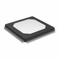
ADSP-21060KS-160 Analog Devices Inc, ADSP-21060KS-160 Datasheet - Page 33

ADSP-21060KS-160
Manufacturer Part Number
ADSP-21060KS-160
Description
Digital Signal Processor IC
Manufacturer
Analog Devices Inc
Series
SHARC®r
Type
Floating Pointr
Datasheets
1.ADSP-21062KSZ-133.pdf
(64 pages)
2.ADSP-21060KS-160.pdf
(47 pages)
3.ADSP-21060KS-160.pdf
(64 pages)
Specifications of ADSP-21060KS-160
Supply Voltage Max
5.25V
Dsp Type
Fixed / Floating Point
Mounting Type
Surface Mount
Package / Case
240-MQFP
Memory Organization - Ram
4M
Rohs Status
RoHS non-compliant
Interface
Host Interface, Link Port, Serial Port
Clock Rate
40MHz
Non-volatile Memory
External
On-chip Ram
512kB
Voltage - I/o
5.00V
Voltage - Core
5.00V
Operating Temperature
0°C ~ 85°C
Device Core Size
32b
Architecture
Super Harvard
Format
Floating Point
Clock Freq (max)
40MHz
Mips
40
Device Input Clock Speed
40MHz
Ram Size
512KB
Operating Supply Voltage (typ)
5V
Operating Supply Voltage (min)
4.75V
Operating Supply Voltage (max)
5.25V
Operating Temp Range
0C to 85C
Operating Temperature Classification
Commercial
Mounting
Surface Mount
Pin Count
240
Package Type
MQFP
Lead Free Status / Rohs Status
Not Compliant
Available stocks
Company
Part Number
Manufacturer
Quantity
Price
Company:
Part Number:
ADSP-21060KS-160
Manufacturer:
AD
Quantity:
5 510
Company:
Part Number:
ADSP-21060KS-160
Manufacturer:
SHARP
Quantity:
5 510
Company:
Part Number:
ADSP-21060KS-160
Manufacturer:
Analog Devices Inc
Quantity:
10 000
Link Ports: 2 × CLK Speed Operation
Calculation of link receiver data setup and hold relative to link clock is required to determine the maximum allowable skew that can
be introduced in the transmission path between LDATA and LCLK. Setup skew is the maximum delay that can be introduced in
LDATA relative to LCLK, (setup skew = t
duced in LCLK relative to LDATA, (hold skew = t
specifications will result in unrealistically small skew times because they include multiple tester guardbands. The setup and hold skew
times shown below are calculated to include only one tester guardband.
Parameter
Receive
Timing Requirements:
t
t
t
t
t
Switching Characteristics:
t
t
Transmit
Timing Requirements:
t
t
Switching Characteristics:
t
t
t
t
t
t
NOTE
1
SLDCL
HLDCL
LCLKIW
LCLKRWL
LCLKRWH
DLAHC
DLALC
SLACH
HLACH
DLCLK
DLDCH
HLDCH
LCLKTWL
LCLKTWH
DLACLK
LACK will go low with t
ADSP-21060 Setup Skew
ADSP-21060 Hold Skew
ADSP-21060L Setup Skew = 1.87 ns max
ADSP-21060L Hold Skew = 1.69 ns max
Data Setup before LCLK Low
Data Hold after LCLK Low
LCLK Period (2 × Operation)
LCLK Width Low
LCLK Width High
LACK High Delay after CLKIN High
LACK Low Delay after LCLK High
LACK Setup before LCLK High
LACK Hold after LCLK High
LCLK Delay after CLKIN
Data Delay after LCLK High
Data Hold after LCLK High
LCLK Width Low
LCLK Width High
LCLK Low Delay after LACK High
DLALC
relative to rising edge of LCLK after first nibble is received. LACK will not go low if the receiver’s link buffer is not about to fill.
= 1.93 ns max
= 2.95 ns max
LCLKTWH
1
LCLKTWL
min – t
Min
2.5
2.25
t
4.5
4.25
18 + DT/2
6
19
–6.75
–2.0
(t
(t
(t
CK
CK
CK
CK
/2
/4) – 1
/4) – 1
/4) + 9
ADSP-21060
DLDCH
min – t
– t
HLDCH
Max
28.5 + DT/2
16
(t
(t
(3
8
2.5
SLDCL
CK
CK
*
/4) + 1
/4) + 1
t
CK
). Hold skew is the maximum delay that can be intro-
– t
/4) + 16.5
HLDCL
). Calculations made directly from 2 × speed
ADSP-21060/ADSP-21060L
Min
2.25
2.25
t
5.0
4.0
18 + DT/2
6
19
–6.5
–2.0
(t
(t
(t
CK
CK
CK
CK
ADSP-21060L
/2
/4) – 0.75 (t
/4) – 1.5 (t
/4) + 9
Max
18
8
2.25
(3
29.5 + DT/2
CK
CK
*
/4) + 1.5
/4) + 1
t
CK
/4) + 16.5
Units
ns
ns
ns
ns
ns
ns
ns
ns
ns
ns
ns
ns
ns
ns
ns


