ADUC7126BSTZ126-RL Analog Devices Inc, ADUC7126BSTZ126-RL Datasheet - Page 18
ADUC7126BSTZ126-RL
Manufacturer Part Number
ADUC7126BSTZ126-RL
Description
ARM7 With 12-Bit ADC & DACs, 128kB Flash
Manufacturer
Analog Devices Inc
Series
MicroConverter® ADuC7xxxr
Datasheet
1.ADUC7126BSTZ126.pdf
(104 pages)
Specifications of ADUC7126BSTZ126-RL
Core Processor
ARM7
Core Size
16/32-Bit
Speed
41.78MHz
Connectivity
EBI/EMI, I²C, SPI, UART/USART
Peripherals
POR, PWM, WDT
Number Of I /o
40
Program Memory Size
126KB (126K x 8)
Program Memory Type
FLASH
Ram Size
32K x 8
Voltage - Supply (vcc/vdd)
2.7 V ~ 3.6 V
Data Converters
A/D 12x12b, D/A 4x12b
Oscillator Type
Internal
Operating Temperature
-40°C ~ 125°C
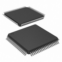
Package / Case
80-LQFP
Lead Free Status / RoHS Status
Lead free / RoHS Compliant
Eeprom Size
-
Lead Free Status / RoHS Status
Lead free / RoHS Compliant
Available stocks
Company
Part Number
Manufacturer
Quantity
Price
Company:

Part Number:
ADUC7126BSTZ126-RL
Manufacturer:
Analog Devices Inc
Quantity:
10 000


ADuC7124/ADuC7126
Table 10. Pin Function Descriptions (ADuC7126 80-Lead LQFP)
Pin No.
1
2
3
4
5
6
7
8
9
10
BM/P0.0/CMP
Mnemonic
ADC4
ADC5
ADC6
ADC7
ADC8
ADC9
ADC10
ADCNEG
DACGND
DACV
DD
OUT
P0.1/PWM4/BLE
DAC0/ADC12
DAC1/ADC13
DAC2/ADC14
DAC3/ADC15
/PLAI[7]/MS0
DACGND
ADCNEG
DACV
XCLKO
ADC10
XCLKI
ADC4
ADC5
ADC6
ADC7
ADC8
ADC9
TMS
TDI
DD
10
12
13
14
15
16
17
18
19
20
11
1
2
3
4
5
6
7
8
9
80 79 78 77 76 75 74 73 72 71 70 69 68 67 66 65 64 63 62 61
21 22 23 24 25 26 27 28 29 30 31 32 33 34 35 36 37 38 39 40
PIN 1
Description
Single-Ended or Differential Analog Input 4.
Single-Ended or Differential Analog Input 5.
Single-Ended or Differential Analog Input 6.
Single-Ended or Differential Analog Input 7.
Single-Ended or Differential Analog Input 8.
Single-Ended or Differential Analog Input 9.
Single-Ended or Differential Analog Input 10.
Bias Point or Negative Analog Input of the ADC in Pseudo Differential Mode. Must be
connected to the ground of the signal to convert. This bias point must be between 0 V
and 1 V.
Ground for the DAC. Typically connected to AGND.
3.3 V Power Supply for the DACs. Must be connected to AV
Figure 8. ADuC7126 Pin Configuration
ADuC7126
Rev. B | Page 18 of 104
TOP VIEW
60
59
58
57
56
55
54
53
52
51
50
49
48
47
46
45
44
43
42
41
P1.3/SPM3/CTS/I2C1SDA/PLAI[3]
P1.4/SPM4/RI/SPICLK/PLAI[4]/IRQ2
P1.5/SPM5/DCD/SPIMISO/PLAI[5]/IRQ3
P4.1/SPM11/SOUT1/AD9/PLAO[9]
P4.0/SPM10/SIN1/AD8/PLAO[8]
P1.6/SPM6/PLAI[6]
P1.7/SPM7/DTR/SPICS/PLAO[0]
P3.7/AD7/PWM
P3.6/AD6/PWM
P2.2/RS/PWM1/PLAO[7]
P2.1/WS/PWM0/PLAO[6]
P2.3/SPM12/AE/SIN1
IOV
IOGND
P0.7/SPM8/ECLK/XCLK/PLAO[4]/SIN0
P2.0/SPM9/PLAO[5]/CONV
P2.7/PWM3/MS3
IRQ1/P0.5/ADC
IRQ0/P0.4/PWM
RST
DD
SYNC
TRIP
BUSY
TRIP
DD
/PLAI[14]
.
/PLAO[1]/MS1
/PLAI[15]
/PLAO[2]/MS2
START
/SOUT0
Related parts for ADUC7126BSTZ126-RL
Image
Part Number
Description
Manufacturer
Datasheet
Request
R

Part Number:
Description:
Precision Analog Microcontroller, 12-Bit Analog I/O, Large Memory, ARM7TDMI MCU with Enhanced IRQ Handler
Manufacturer:
Analog Devices
Datasheet:

Part Number:
Description:
±1.7g Dual-Axis IMEMS Accelerometer Evaluation Board
Manufacturer:
Analog Devices Inc
Datasheet:

Part Number:
Description:
Inertial Sensor Evaluation System
Manufacturer:
Analog Devices Inc
Datasheet:
Part Number:
Description:
Manufacturer:
Analog Devices Inc
Datasheet:
Part Number:
Description:
Manufacturer:
Analog Devices Inc
Datasheet:
Part Number:
Description:
Manufacturer:
Analog Devices Inc
Datasheet:
Part Number:
Description:
Manufacturer:
Analog Devices Inc
Datasheet:
Part Number:
Description:
Manufacturer:
Analog Devices Inc
Datasheet:
Part Number:
Description:
Manufacturer:
Analog Devices Inc
Datasheet:
Part Number:
Description:
Manufacturer:
Analog Devices Inc
Datasheet:
Part Number:
Description:
Manufacturer:
Analog Devices Inc
Datasheet:
Part Number:
Description:
Manufacturer:
Analog Devices Inc
Datasheet:
Part Number:
Description:
Manufacturer:
Analog Devices Inc
Datasheet: