ADUC7126BSTZ126-RL Analog Devices Inc, ADUC7126BSTZ126-RL Datasheet - Page 53
ADUC7126BSTZ126-RL
Manufacturer Part Number
ADUC7126BSTZ126-RL
Description
ARM7 With 12-Bit ADC & DACs, 128kB Flash
Manufacturer
Analog Devices Inc
Series
MicroConverter® ADuC7xxxr
Datasheet
1.ADUC7126BSTZ126.pdf
(104 pages)
Specifications of ADUC7126BSTZ126-RL
Core Processor
ARM7
Core Size
16/32-Bit
Speed
41.78MHz
Connectivity
EBI/EMI, I²C, SPI, UART/USART
Peripherals
POR, PWM, WDT
Number Of I /o
40
Program Memory Size
126KB (126K x 8)
Program Memory Type
FLASH
Ram Size
32K x 8
Voltage - Supply (vcc/vdd)
2.7 V ~ 3.6 V
Data Converters
A/D 12x12b, D/A 4x12b
Oscillator Type
Internal
Operating Temperature
-40°C ~ 125°C
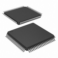
Package / Case
80-LQFP
Lead Free Status / RoHS Status
Lead free / RoHS Compliant
Eeprom Size
-
Lead Free Status / RoHS Status
Lead free / RoHS Compliant
Available stocks
Company
Part Number
Manufacturer
Quantity
Price
Company:

Part Number:
ADUC7126BSTZ126-RL
Manufacturer:
Analog Devices Inc
Quantity:
10 000


DACBKEY1 Register
Name:
Address:
Default Value:
Access:
DACBKEY2 Register
Name:
Address:
Default Value:
Access:
POWER SUPPLY MONITOR
The power supply monitor regulates the IOV
ADuC7124/ADuC7126. It indicates when the IOV
drops below one of two supply trip points. The monitor
function is controlled via the PSMCON register. If enabled in
the IRQEN or FIQEN register, the monitor interrupts the core
using the PSMI bit in the PSMCON MMR. This bit is immediately
cleared when CMP goes high.
This monitor function allows the user to save working registers
to avoid possible data loss due to low supply or brown-out
conditions. It also ensures that normal code execution does not
resume until a safe supply level is established.
PSMCON Register
Name:
Address:
Default Value:
Access:
DACBKEY1
0xFFFF0650
0x0000
Write
DACBKEY2
0xFFFF0658
0x0000
Write
PSMCON
0xFFFF0440
0x0008
Read/write
DD
supply on the
DD
supply pin
Rev. B | Page 53 of 104
Table 68. PSMCON MMR Bit Descriptions
Bit
3
2
1
0
COMPARATOR
The ADuC7124/ADuC7126 integrate a voltage comparator. The
positive input is multiplexed with ADC2, and the negative input
has two options: ADC3 or DAC0. The output of the comparator
can be configured to generate a system interrupt, be routed
directly to the programmable logic array, start an ADC conver-
sion, or be on an external pin, CMP
Hysteresis
Figure 44 shows how the input offset voltage and hysteresis
terms are defined. Input offset voltage (V
between the center of the hysteresis range and the ground level.
This can either be positive or negative. The hysteresis voltage
(V
H
) is ½ the width of the hysteresis range.
Name
CMP
TP
PSMEN
PSMI
P0.0/CMP
ADC2/CMP0
ADC3/CMP1
Figure 44. Comparator Hysteresis Transfer Function
CMP
OUT
Description
Comparator bit. This is a read-only bit that
directly reflects the state of the comparator.
Read 1 indicates that the IOV
its selected trip point or that the PSM is in
power-down mode. Read 0 indicates that the
IOV
bit should be set before leaving the interrupt
service routine.
Trip point selection bits.
0 = 2.79 V, 1 = 3.07 V.
Power supply monitor enable bit.
Set to 1 to enable the power supply monitor
circuit.
Clear to 0 to disable the power supply monitor
circuit.
Power supply monitor interrupt bit. This bit is set
high by the MicroConverter when CMP goes low,
indicating low I/O supply. The PSMI bit can be
used to interrupt the processor. When CMP
returns high, the PSMI bit can be cleared by
writing a 1 to this location. A 0 write has no
effect. There is no timeout delay; PSMI can be
immediately cleared when CMP goes high.
OUT
DD
DAC0
supply is below its selected trip point. This
V
Figure 43. Comparator
OS
V
H
MUX
ADuC7124/ADuC7126
V
H
OUT
, as shown in Figure 43.
OS
COMP0
) is the difference
DD
MUX
supply is above
IRQ
Related parts for ADUC7126BSTZ126-RL
Image
Part Number
Description
Manufacturer
Datasheet
Request
R

Part Number:
Description:
Precision Analog Microcontroller, 12-Bit Analog I/O, Large Memory, ARM7TDMI MCU with Enhanced IRQ Handler
Manufacturer:
Analog Devices
Datasheet:

Part Number:
Description:
±1.7g Dual-Axis IMEMS Accelerometer Evaluation Board
Manufacturer:
Analog Devices Inc
Datasheet:

Part Number:
Description:
Inertial Sensor Evaluation System
Manufacturer:
Analog Devices Inc
Datasheet:
Part Number:
Description:
Manufacturer:
Analog Devices Inc
Datasheet:
Part Number:
Description:
Manufacturer:
Analog Devices Inc
Datasheet:
Part Number:
Description:
Manufacturer:
Analog Devices Inc
Datasheet:
Part Number:
Description:
Manufacturer:
Analog Devices Inc
Datasheet:
Part Number:
Description:
Manufacturer:
Analog Devices Inc
Datasheet:
Part Number:
Description:
Manufacturer:
Analog Devices Inc
Datasheet:
Part Number:
Description:
Manufacturer:
Analog Devices Inc
Datasheet:
Part Number:
Description:
Manufacturer:
Analog Devices Inc
Datasheet:
Part Number:
Description:
Manufacturer:
Analog Devices Inc
Datasheet:
Part Number:
Description:
Manufacturer:
Analog Devices Inc
Datasheet: