ADUC7126BSTZ126-RL Analog Devices Inc, ADUC7126BSTZ126-RL Datasheet - Page 55
ADUC7126BSTZ126-RL
Manufacturer Part Number
ADUC7126BSTZ126-RL
Description
ARM7 With 12-Bit ADC & DACs, 128kB Flash
Manufacturer
Analog Devices Inc
Series
MicroConverter® ADuC7xxxr
Datasheet
1.ADUC7126BSTZ126.pdf
(104 pages)
Specifications of ADUC7126BSTZ126-RL
Core Processor
ARM7
Core Size
16/32-Bit
Speed
41.78MHz
Connectivity
EBI/EMI, I²C, SPI, UART/USART
Peripherals
POR, PWM, WDT
Number Of I /o
40
Program Memory Size
126KB (126K x 8)
Program Memory Type
FLASH
Ram Size
32K x 8
Voltage - Supply (vcc/vdd)
2.7 V ~ 3.6 V
Data Converters
A/D 12x12b, D/A 4x12b
Oscillator Type
Internal
Operating Temperature
-40°C ~ 125°C
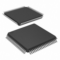
Package / Case
80-LQFP
Lead Free Status / RoHS Status
Lead free / RoHS Compliant
Eeprom Size
-
Lead Free Status / RoHS Status
Lead free / RoHS Compliant
Available stocks
Company
Part Number
Manufacturer
Quantity
Price
Company:

Part Number:
ADUC7126BSTZ126-RL
Manufacturer:
Analog Devices Inc
Quantity:
10 000


External Crystal Selection
To switch to an external crystal, the user must follow this
procedure:
1.
2.
3.
4.
Example source code:
//enable T2 interrupt
In noisy environments, noise can couple to the external crystal
pins, and PLL may lose lock momentarily. A PLL interrupt is
provided in the interrupt controller. The core clock is immediately
halted, and this interrupt is serviced only when the lock is restored.
In case of crystal loss, the watchdog timer should be used. During
initialization, a test on the RSTSTA can determine if the reset
came from the watchdog timer.
Table 70. Operating Modes
Mode
Active
Pause
Nap
Sleep
Stop
Table 71. Typical Current Consumption at 25°C in mA, V
Mode
Active
Pause
Nap
Sleep
Stop
IRQEN = 0x10;
PLLKEY1 = 0xAA;
PLLCON = 0x01;
PLLKEY2 = 0x55;
POWKEY1 = 0x01;
POWCON0 = 0x27;
POWKEY2 = 0xF4;
Enable the Timer2 interrupt and configure it for a timeout
period of >120 µs.
Follow the write sequence to the PLLCON register, setting
the MDCLK bits to 01 and clearing the OSEL bit.
Force the part into nap mode by following the correct write
sequence to the POWCON0 register.
When the part is interrupted from nap mode by the
Timer2 interrupt source, the clock source has switched to
the external clock.
T2LD = 5;
T2CON = 0x480;
Core
On
CD = 0
33.3
20.6
4.6
0.2
0.2
Peripherals
On
On
// Set core into nap mode
CD = 1
23.1
12.7
4.6
0.2
0.2
PLL
On
On
On
CD = 2
15.4
8.8
4.6
0.2
0.2
XTAL/T2/T3
On
On
On
On
Rev. B | Page 55 of 104
DD
CD = 3
11.6
6.8
4.6
0.2
0.2
= 3.3 V
External Clock Selection
To switch to an external clock on P0.7, configure P0.7 in
Mode 1. The external clock can be up to 41.78 MHz, providing
the tolerance is 1%.
Example source code:
//enable T2 interrupt
Set core into nap mode
Power Control System
A choice of operating modes is available on the ADuC7124/
ADuC7126. Table 70 describes what part is powered on in the
different modes and indicates the power-up time.
Table 71 gives some typical values of the total current
consumption (analog + digital supply currents) in the different
modes, depending on the clock divider bits. The AC, DAC, I
and SPI are turned off.
IRQ0 to IRQ3
On
On
On
On
On
IRQEN = 0x10;
PLLKEY1 = 0xAA;
PLLCON = 0x03; //Select external clock
PLLKEY2 = 0x55;
POWKEY1 = 0x01;
POWCON0 = 0x27;
POWKEY2 = 0xF4;
CD = 4
9.7
5.8
4.6
0.2
0.2
T2LD = 5;
T2CON = 0x480;
CD = 5
8.8
5.3
4.6
0.2
0.2
Start-Up/Power-On Time
66 ms at CD = 0
2.6 µs at CD = 0; 247 µs at CD = 7
2.6 µs at CD = 0; 247 µs at CD = 7
1.58 ms
1.7 ms
ADuC7124/ADuC7126
CD = 6
8.3
5.1
4.6
0.2
0.2
CD = 7
8.1
4.9
4.6
0.2
0.2
//
2
C,
Related parts for ADUC7126BSTZ126-RL
Image
Part Number
Description
Manufacturer
Datasheet
Request
R

Part Number:
Description:
Precision Analog Microcontroller, 12-Bit Analog I/O, Large Memory, ARM7TDMI MCU with Enhanced IRQ Handler
Manufacturer:
Analog Devices
Datasheet:

Part Number:
Description:
±1.7g Dual-Axis IMEMS Accelerometer Evaluation Board
Manufacturer:
Analog Devices Inc
Datasheet:

Part Number:
Description:
Inertial Sensor Evaluation System
Manufacturer:
Analog Devices Inc
Datasheet:
Part Number:
Description:
Manufacturer:
Analog Devices Inc
Datasheet:
Part Number:
Description:
Manufacturer:
Analog Devices Inc
Datasheet:
Part Number:
Description:
Manufacturer:
Analog Devices Inc
Datasheet:
Part Number:
Description:
Manufacturer:
Analog Devices Inc
Datasheet:
Part Number:
Description:
Manufacturer:
Analog Devices Inc
Datasheet:
Part Number:
Description:
Manufacturer:
Analog Devices Inc
Datasheet:
Part Number:
Description:
Manufacturer:
Analog Devices Inc
Datasheet:
Part Number:
Description:
Manufacturer:
Analog Devices Inc
Datasheet:
Part Number:
Description:
Manufacturer:
Analog Devices Inc
Datasheet:
Part Number:
Description:
Manufacturer:
Analog Devices Inc
Datasheet: