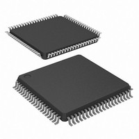
ADUC7126BSTZ126-RL Analog Devices Inc, ADUC7126BSTZ126-RL Datasheet - Page 92

ADUC7126BSTZ126-RL
Manufacturer Part Number
ADUC7126BSTZ126-RL
Description
ARM7 With 12-Bit ADC & DACs, 128kB Flash
Manufacturer
Analog Devices Inc
Series
MicroConverter® ADuC7xxxr
Datasheet
1.ADUC7126BSTZ126.pdf
(104 pages)
Specifications of ADUC7126BSTZ126-RL
Core Processor
ARM7
Core Size
16/32-Bit
Speed
41.78MHz
Connectivity
EBI/EMI, I²C, SPI, UART/USART
Peripherals
POR, PWM, WDT
Number Of I /o
40
Program Memory Size
126KB (126K x 8)
Program Memory Type
FLASH
Ram Size
32K x 8
Voltage - Supply (vcc/vdd)
2.7 V ~ 3.6 V
Data Converters
A/D 12x12b, D/A 4x12b
Oscillator Type
Internal
Operating Temperature
-40°C ~ 125°C
Package / Case
80-LQFP
Lead Free Status / RoHS Status
Lead free / RoHS Compliant
Eeprom Size
-
Lead Free Status / RoHS Status
Lead free / RoHS Compliant
Available stocks
Company
Part Number
Manufacturer
Quantity
Price
Company:
Part Number:
ADUC7126BSTZ126-RL
Manufacturer:
Analog Devices Inc
Quantity:
10 000
ADuC7124/ADuC7126
Table 140. T0CON MMR Bit Descriptions
Bit
[31:8]
7
6
[5:4]
[3:2]
[1:0]
T0CLRI Register
Name:
Address:
Default Value:
Access:
T0CLRI is an 8-bit register. Writing any value to this register
clears the interrupt.
Timer1 (General-Purpose Timer)
Timer1 is a general-purpose, 32-bit timer (count down or count
up) with a programmable prescaler. The source can be the 32 kHz
external crystal, the undivided system, the core clock, or P1.1
(maximum frequency 41.78 MHz). This source can be scaled by
a factor of 1, 16, 256, or 32,768.
The counter can be formatted as a standard 32-bit value or as
hours: minutes: seconds: hundredths.
Timer1 has a capture register (T1CAP) that can be triggered by
a selected IRQ source initial assertion. This feature can be used
to determine the assertion of an event more accurately than the
precision allowed by the RTOS timer when the IRQ is serviced.
Timer1 can be used to start ADC conversions.
Value
00
01
10
11
00
01
10
11
Description
Reserved.
Timer0 enable bit.
Set by the user to enable Timer0.
Cleared by the user to disable Timer0 by
default.
Timer0 mode.
Set by the user to operate in periodic mode.
Cleared by the user to operate in free-running
mode. Default mode.
Clock select bits.
HCLK.
UCLK.
32.768 kHz.
Reserved.
Prescale.
Core clock/1. Default value.
Core clock/16.
Core clock/256.
Undefined. Equivalent to 00.
Reserved.
T0CLRI
0xFFFF030C
0xFF
Write only
Rev. B | Page 92 of 104
32kHz OSCILLATOR
The Timer1 interface consists of five MMRs: T1LD, T1VAL,
T1CON, T1CLRI, and T1CAP.
T1LD Register
Name:
Address:
Default Value:
Access:
T1LD is a 32-bit load register.
T1VAL Register
Name:
Address:
Default Value:
Access:
T1VAL is a 32-bit read-only register that represents the current
state of the counter.
T1CON Register
Name:
Address:
Default Value:
Access:
T1CON is the configuration MMR described in Table 141.
HCLK
UCLK
P1.0
Figure 54. Timer1 Block Diagram
T1LD
0xFFFF0320
0x00000000
Read/write
T1VAL
0xFFFF0324
0xFFFFFFFF
Read only
T1CON
0xFFFF0328
0x0000
Read/write
IRQ[19:0]
PRESCALER
÷1, 16, 256,
OR 32,768
UP/DOWN
COUNTER
CAPTURE
32-BIT
32-BIT
LOAD
TIMER1
VALUE
TIMER1 IRQ
ADC CONVERSION


