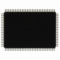
CY7C1471V33-133AXC Cypress Semiconductor Corp, CY7C1471V33-133AXC Datasheet - Page 12

CY7C1471V33-133AXC
Manufacturer Part Number
CY7C1471V33-133AXC
Description
SRAM (Static RAM)
Manufacturer
Cypress Semiconductor Corp
Datasheet
1.CY7C1471V33-133AXC.pdf
(36 pages)
Specifications of CY7C1471V33-133AXC
Format - Memory
RAM
Memory Type
SRAM - Synchronous
Memory Size
72M (2M x 36)
Speed
133MHz
Interface
Parallel
Voltage - Supply
3.135 V ~ 3.6 V
Operating Temperature
0°C ~ 70°C
Package / Case
100-LQFP
Density
72Mb
Access Time (max)
6.5ns
Sync/async
Synchronous
Architecture
SDR
Clock Freq (max)
133MHz
Operating Supply Voltage (typ)
3.3V
Address Bus
21b
Package Type
TQFP
Operating Temp Range
0C to 70C
Number Of Ports
4
Supply Current
305mA
Operating Supply Voltage (min)
3.135V
Operating Supply Voltage (max)
3.6V
Operating Temperature Classification
Commercial
Mounting
Surface Mount
Pin Count
100
Word Size
36b
Number Of Words
2M
Lead Free Status / RoHS Status
Lead free / RoHS Compliant
Lead Free Status / RoHS Status
Lead free / RoHS Compliant
Other names
428-2167
CY7C1471V33-133AXC
CY7C1471V33-133AXC
Available stocks
Company
Part Number
Manufacturer
Quantity
Price
Company:
Part Number:
CY7C1471V33-133AXC
Manufacturer:
Cypress Semiconductor Corp
Quantity:
135
Company:
Part Number:
CY7C1471V33-133AXC
Manufacturer:
TOSHIBA
Quantity:
2 100
Company:
Part Number:
CY7C1471V33-133AXC
Manufacturer:
Cypress Semiconductor Corp
Quantity:
10 000
Part Number:
CY7C1471V33-133AXC
Manufacturer:
CYPRESS/赛普拉斯
Quantity:
20 000
Company:
Part Number:
CY7C1471V33-133AXCT
Manufacturer:
Cypress Semiconductor Corp
Quantity:
10 000
CY7C1475V33 provides Byte Write capability that is described
in the
with the selected BW
bytes. Bytes not selected during a byte write operation remain
unaltered. A synchronous self timed write mechanism has been
provided to simplify the write operations. Byte write capability is
included to greatly simplify read/modify/write sequences, which
can be reduced to simple byte write operations.
Because
CY7C1475V33 are common IO devices, data must not be driven
into the device while the outputs are active. The output enable
(OE) can be deasserted HIGH before presenting data to the DQs
and DQP
safety precaution, DQs and DQP
during the data portion of a write cycle, regardless of the state of
OE.
Burst Write Accesses
The CY7C1471V33, CY7C1473V33, and CY7C1475V33 have
an on-chip burst counter that enables the user to supply a single
address and conduct up to four write operations without
reasserting the address inputs. ADV/LD must be driven LOW to
load the initial address, as described in the
Accesses
subsequent clock rise, the chip enables (CE
and WE inputs are ignored and the burst counter is incremented.
The correct BW
write to write the correct bytes of data.
Sleep Mode
The ZZ input pin is an asynchronous input. Asserting ZZ places
the SRAM in a power conservation “sleep” mode. Two clock
cycles are required to enter into or exit from this “sleep” mode.
While in this mode, data integrity is guaranteed. Accesses
pending when entering the “sleep” mode are not considered valid
nor is the completion of the operation guaranteed. The device
must be deselected before entering the “sleep” mode. CE
and CE
ZZ input returns LOW.
ZZ Mode Electrical Characteristics
Document Number: 38-05288 Rev. *L
I
t
t
t
t
DDZZ
ZZS
ZZREC
ZZI
RZZI
Parameter
“Truth Table for Read/Write” on page
3
, must remain inactive for the duration of t
X
section. When ADV/LD is driven HIGH on the
inputs. Doing so tri-states the output drivers. As a
the
X
inputs must be driven in each cycle of the burst
Sleep mode standby current
Device operation to ZZ
ZZ recovery time
ZZ active to sleep current
ZZ Inactive to exit sleep current
CY7C1471V33,
X
input selectively writes to only the desired
Description
X
are automatically tri-stated
CY7C1473V33,
14. The input WE
1
, CE
ZZREC
Single Write
2
, and CE
after the
1
, CE
and
3
2
)
,
ZZ > V
ZZ > V
ZZ < 0.2V
This parameter is sampled
This parameter is sampled
Interleaved Burst Address Table
(MODE = Floating or V
Linear Burst Address Table
(MODE = GND)
Test Conditions
DD
DD
Address
Address
A1: A0
A1: A0
– 0.2 V
– 0.2 V
First
First
00
01
10
00
01
10
11
11
Address
Address
Second
Second
A1: A0
A1: A0
01
00
11
10
01
10
11
00
2t
Min
CYC
–
–
–
0
DD
Address
Address
A1: A0
A1: A0
)
Third
Third
10
00
01
10
00
01
11
11
2t
2t
CY7C1471V33
CY7C1473V33
CY7C1475V33
Max
120
CYC
CYC
–
–
Address
Address
Page 12 of 36
Fourth
A1: A0
Fourth
A1: A0
Unit
mA
ns
ns
ns
ns
11
10
01
00
11
00
01
10
[+] Feedback


