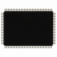
CY7C1471V33-133AXC Cypress Semiconductor Corp, CY7C1471V33-133AXC Datasheet - Page 14

CY7C1471V33-133AXC
Manufacturer Part Number
CY7C1471V33-133AXC
Description
SRAM (Static RAM)
Manufacturer
Cypress Semiconductor Corp
Datasheet
1.CY7C1471V33-133AXC.pdf
(36 pages)
Specifications of CY7C1471V33-133AXC
Format - Memory
RAM
Memory Type
SRAM - Synchronous
Memory Size
72M (2M x 36)
Speed
133MHz
Interface
Parallel
Voltage - Supply
3.135 V ~ 3.6 V
Operating Temperature
0°C ~ 70°C
Package / Case
100-LQFP
Density
72Mb
Access Time (max)
6.5ns
Sync/async
Synchronous
Architecture
SDR
Clock Freq (max)
133MHz
Operating Supply Voltage (typ)
3.3V
Address Bus
21b
Package Type
TQFP
Operating Temp Range
0C to 70C
Number Of Ports
4
Supply Current
305mA
Operating Supply Voltage (min)
3.135V
Operating Supply Voltage (max)
3.6V
Operating Temperature Classification
Commercial
Mounting
Surface Mount
Pin Count
100
Word Size
36b
Number Of Words
2M
Lead Free Status / RoHS Status
Lead free / RoHS Compliant
Lead Free Status / RoHS Status
Lead free / RoHS Compliant
Other names
428-2167
CY7C1471V33-133AXC
CY7C1471V33-133AXC
Available stocks
Company
Part Number
Manufacturer
Quantity
Price
Company:
Part Number:
CY7C1471V33-133AXC
Manufacturer:
Cypress Semiconductor Corp
Quantity:
135
Company:
Part Number:
CY7C1471V33-133AXC
Manufacturer:
TOSHIBA
Quantity:
2 100
Company:
Part Number:
CY7C1471V33-133AXC
Manufacturer:
Cypress Semiconductor Corp
Quantity:
10 000
Part Number:
CY7C1471V33-133AXC
Manufacturer:
CYPRESS/赛普拉斯
Quantity:
20 000
Company:
Part Number:
CY7C1471V33-133AXCT
Manufacturer:
Cypress Semiconductor Corp
Quantity:
10 000
Truth Table for Read/Write
The read-write truth table for CY7C1471V33 follows.
Truth Table for Read/Write
The read-write truth table for CY7C1473V33 follows.
Notes
Document Number: 38-05288 Rev. *L
Read
Write no bytes written
Write byte A – (DQ
Write byte B – (DQ
Write byte C – (DQ
Write byte D – (DQ
Write all bytes
Truth Table for Read/Write
The read-write truth table for CY7C1475V33 follows.
Read
Write – no bytes written
Write byte X(DQ
Write all bytes
9. X = “Don't Care.” H = Logic HIGH, L = Logic LOW. BW
10. Write is defined by BW
11. Table only lists a partial listing of the byte write combinations. Any combination of BW
Read
Write – no bytes written
Write byte a – (DQ
Write byte b – (DQ
Write both bytes
selects are asserted, see
x
B
C
D
A
a
b
and DQP
X
and DQP
and DQP
and DQP
and DQP
and DQP
and DQP
Function
, and WE. See
“Truth Table for Read/Write” on page 14
x)
Function
Function
B
D
A
C
a
b
)
)
)
)
)
)
“Truth Table for Read/Write” on page
X
= L signifies at least one byte write select is active, BW
[9, 10, 11]
[9, 10, 11]
[9, 10, 11]
for details.
WE
H
L
L
L
L
L
L
14.
X
is valid. Appropriate write is based on which byte write is active.
BW
H
H
H
H
X
L
L
A
WE
H
L
L
L
L
WE
BW
H
L
L
L
X
H
H
H
H
L
L
X
B
= valid signifies that the desired byte write
BW
X
H
H
L
L
b
BW
X
H
H
H
H
L
L
C
CY7C1471V33
CY7C1473V33
CY7C1475V33
All BW = L
BW
BW
X
H
H
X
H
L
L
L
BW
Page 14 of 36
a
x
X
H
H
H
H
L
L
D
[+] Feedback


