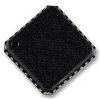
ADAU1961WBCPZ Analog Devices Inc, ADAU1961WBCPZ Datasheet - Page 13

ADAU1961WBCPZ
Manufacturer Part Number
ADAU1961WBCPZ
Description
IC STEREO AUD CODEC LP 32LFCSP
Manufacturer
Analog Devices Inc
Type
Audio Codecr
Datasheet
1.ADAU1961WBCPZ-RL.pdf
(76 pages)
Specifications of ADAU1961WBCPZ
Data Interface
Serial
Resolution (bits)
24 b
Number Of Adcs / Dacs
2 / 2
Sigma Delta
No
S/n Ratio, Adcs / Dacs (db) Typ
99 / 101
Dynamic Range, Adcs / Dacs (db) Typ
99 / 101
Voltage - Supply, Analog
2.97 V ~ 3.63 V
Operating Temperature
-40°C ~ 105°C
Mounting Type
Surface Mount
Package / Case
32-VFQFN, CSP Exposed Pad
Audio Codec Type
Stereo
No. Of Adcs
2
No. Of Dacs
2
No. Of Input Channels
2
No. Of Output Channels
2
Adc / Dac Resolution
24bit
Adcs / Dacs Signal To Noise Ratio
101dB
Sampling Rate
96kSPS
No. Of
RoHS Compliant
Rohs Compliant
Yes
Lead Free Status / RoHS Status
Lead free / RoHS Compliant
Available stocks
Company
Part Number
Manufacturer
Quantity
Price
Company:
Part Number:
ADAU1961WBCPZ
Manufacturer:
AD
Quantity:
2 469
Part Number:
ADAU1961WBCPZ
Manufacturer:
ADI/亚德诺
Quantity:
20 000
PIN CONFIGURATION AND FUNCTION DESCRIPTIONS
Table 9. Pin Function Descriptions
Pin No.
1
2
3
4
5
6
7
8
9
10
11
12
13
14
15
16
17
18
Mnemonic
IOVDD
MCLK
ADDR0/CLATCH
JACKDET/MICIN
MICBIAS
LAUX
CM
AVDD
AGND
LINP
LINN
RINP
RINN
RAUX
ROUTP
ROUTN
LOUTN
LOUTP
Type
PWR
D_IN
D_IN
D_IN
A_OUT
A_IN
A_OUT
PWR
PWR
A_IN
A_IN
A_IN
A_IN
A_IN
A_OUT
A_OUT
A_OUT
A_OUT
1
ADDR0/CLATCH
JACKDET/MICIN
NOTES
1. THE EXPOSED PAD IS CONNECTED INTERNALLY TO THE
ADAU1961 GROUNDS. FOR INCREASED RELIABILITY OF THE
SOLDER JOINTS AND MAXIMUM THERMAL CAPABILITY, IT IS
RECOMMENDED THAT THE PAD BE SOLDERED TO THE
GROUND PLANE.
Description
Supply for Digital Input and Output Pins. The digital output pins are supplied from IOVDD,
which also sets the highest input voltage that should be seen on the digital input pins.
IOVDD should be set to 3.3 V. The current draw of this pin is variable because it is dependent
on the loads of the digital outputs. IOVDD should be decoupled to DGND with a 100 nF
capacitor and a 10 μF capacitor.
External Master Clock Input.
SPI Latch Signal (CLATCH). Must go low at the beginning of an SPI transaction and high at the
end of a transaction. Each SPI transaction can take a different number of CCLKs to complete,
depending on the address and read/write bit that are sent at the beginning of the SPI
transaction.
Detect Insertion/Removal of Headphone Plug (JACKDET).
Digital Microphone Stereo Input (MICIN).
Bias Voltage for Electret Microphone.
Left Channel Single-Ended Auxiliary Input. Biased at AVDD/2.
AVDD/2 V Common-Mode Reference. A 10 μF to 47 μF standard decoupling capacitor should
be connected between this pin and AGND to reduce crosstalk between the ADCs and DACs.
This pin can be used to bias external analog circuits, as long as they are not drawing current
from CM (for example, the noninverting input of an op amp).
3.3 V Analog Supply for DAC and Microphone Bias. This pin should be decoupled locally to
AGND with a 100 nF capacitor.
Analog Ground. The AGND and DGND pins can be tied together on a common ground plane.
AGND should be decoupled locally to AVDD with a 100 nF capacitor.
Left Channel Noninverting Input or Single-Ended Input 0. Biased at AVDD/2.
Left Channel Inverting Input or Single-Ended Input 1. Biased at AVDD/2.
Right Channel Noninverting Input or Single-Ended Input 2. Biased at AVDD/2.
Right Channel Inverting Input or Single-Ended Input 3. Biased at AVDD/2.
Left Line Output, Negative. Biased at AVDD/2.
Left Line Output, Positive. Biased at AVDD/2.
I
Right Channel Single-Ended Auxiliary Input. Biased at AVDD/2.
Right Line Output, Positive. Biased at AVDD/2.
Right Line Output, Negative. Biased at AVDD/2.
2
C Address Bit 0 (ADDR0).
MICBIAS
IOVDD
MCLK
AVDD
LAUX
CM
1
2
3
4
5
6
7
8
Figure 7. Pin Configuration
Rev. 0 | Page 13 of 76
ADAU1961
(Not to Scale)
PIN 1
INDICATOR
TOP VIEW
24 DVDDOUT
23 AVDD
22 AGND
21 MONOOUT
20 LHP
19 RHP
18 LOUTP
17 LOUTN
ADAU1961


