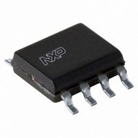
PHC21025,118 NXP Semiconductors, PHC21025,118 Datasheet - Page 9

PHC21025,118
Manufacturer Part Number
PHC21025,118
Description
MOSFET N/P-CH 30V SOT96-1
Manufacturer
NXP Semiconductors
Datasheet
1.PHC21025118.pdf
(16 pages)
Specifications of PHC21025,118
Fet Type
N and P-Channel
Fet Feature
Logic Level Gate
Rds On (max) @ Id, Vgs
100 mOhm @ 2.2A, 10V
Drain To Source Voltage (vdss)
30V
Current - Continuous Drain (id) @ 25° C
3.5A, 2.3A
Vgs(th) (max) @ Id
2.8V @ 1mA
Gate Charge (qg) @ Vgs
30nC @ 10V
Input Capacitance (ciss) @ Vds
250pF @ 20V
Power - Max
2W
Mounting Type
Surface Mount
Package / Case
8-SOIC (3.9mm Width)
Configuration
Dual Dual Drain
Transistor Polarity
N and P-Channel
Resistance Drain-source Rds (on)
0.1 Ohms
Drain-source Breakdown Voltage
30 V
Gate-source Breakdown Voltage
+/- 20 V
Continuous Drain Current
3.5 A, - 2.3 A
Power Dissipation
2 W
Maximum Operating Temperature
+ 150 C
Mounting Style
SMD/SMT
Minimum Operating Temperature
- 65 C
Lead Free Status / RoHS Status
Lead free / RoHS Compliant
Other names
934034320118
PHC21025 /T3
PHC21025 /T3
PHC21025 /T3
PHC21025 /T3
NXP Semiconductors
PHC21025
Product data sheet
Fig 9.
Fig 11. Gate-source voltage as a function of gate
V
(V)
(A)
I
GS
D
16
12
10
8
4
0
8
6
4
2
0
function of gate-source voltage; N-channel;
typical values
charge; N-channel; typical values
Transfer characteristics: drain current as a
0
0
2
2
4
4
6
6
All information provided in this document is subject to legal disclaimers.
Q
V
G
GS
mbe141
mbe136
(nC)
(V)
Rev. 04 — 17 March 2011
8
8
Fig 10. Transfer characteristics: drain current as a
Fig 12. Gate-source voltage as a function of gate
V
(V)
(A)
I
GS
−10
−10
D
−8
−6
−4
−2
−8
−6
−4
−2
0
0
function of gate-source voltage; P-channel;
typical values
charge; P-channel; typical values
0
0
Complementary intermediate level FET
−2
−2
−4
−4
−6
PHC21025
−6
© NXP B.V. 2011. All rights reserved.
−8
V
Q
GS
g
mbe157
mbe145
(nC)
(V)
−10
−8
9 of 16


