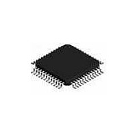
ispPAC-CLK5304S-01TN48I Lattice, ispPAC-CLK5304S-01TN48I Datasheet - Page 37

ispPAC-CLK5304S-01TN48I
Manufacturer Part Number
ispPAC-CLK5304S-01TN48I
Description
Clock Drivers & Distribution ISP 0 Delay Unv Fan- Out Buf-Sngl End I
Manufacturer
Lattice
Type
Zero Delay Programmable PLL Clock Generatorr
Datasheet
1.ISPPAC-CLK5308S-01TN48C.pdf
(56 pages)
Specifications of ispPAC-CLK5304S-01TN48I
Max Input Freq
267 MHz
Minimum Operating Temperature
- 40 C
Mounting Style
SMD/SMT
Supply Voltage (max)
3.6 V
Supply Voltage (min)
3 V
Maximum Operating Temperature
+ 85 C
Package / Case
TQFP-48
Lead Free Status / RoHS Status
Lead free / RoHS Compliant
Available stocks
Company
Part Number
Manufacturer
Quantity
Price
Company:
Part Number:
ISPPAC-CLK5304S-01TN48I
Manufacturer:
Lattice Semiconductor Corporation
Quantity:
10 000
Lattice Semiconductor
Figure 32. ispClock5300S TAP Registers
TAP Controller Specifics
The TAP is controlled by the Test Clock (TCK) and Test Mode Select (TMS) inputs. These inputs determine whether
an Instruction Register or Data Register operation is performed. Driven by the TCK input, the TAP consists of a
small 16-state controller design. In a given state, the controller responds according to the level on the TMS input as
shown in Figure 33. Test Data In (TDI) and TMS are latched on the rising edge of TCK, with Test Data Out (TDO)
becoming valid on the falling edge of TCK. There are six steady states within the controller: Test-Logic-Reset, Run-
Test/Idle, Shift-Data-Register, Pause-Data-Register, Shift-Instruction-Register and Pause-Instruction-Register. But
there is only one steady state for the condition when TMS is set high: the Test-Logic-Reset state. This allows a
reset of the test logic within five TCKs or less by keeping the TMS input high. Test-Logic-Reset is the power-on
default state.
TDI
(42 Bits for ispClock5312S, 5308S 5304S,
(34 Bits for ispClock5312S, 5308S, 5304S,
61 Bits for ispClock5320S and 5316S)
Test Acess Port (TAP)
50 Bits for ispClock5320S and 5316S)
TCK
Instruction Register (8 Bits)
IDCODE Register (32 Bits)
Address Register (10 Bits)
Boundary Scan Register
Bypass Register (1 Bit)
UES Register (32 Bits)
Logic
Data Register
TMS
37
Output
Latch
TDO
ispClock5300S Family Data Sheet
Non-Volatile
E
Memory
2
CMOS


