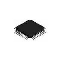
ispPAC-CLK5304S-01TN48I Lattice, ispPAC-CLK5304S-01TN48I Datasheet - Page 8

ispPAC-CLK5304S-01TN48I
Manufacturer Part Number
ispPAC-CLK5304S-01TN48I
Description
Clock Drivers & Distribution ISP 0 Delay Unv Fan- Out Buf-Sngl End I
Manufacturer
Lattice
Type
Zero Delay Programmable PLL Clock Generatorr
Datasheet
1.ISPPAC-CLK5308S-01TN48C.pdf
(56 pages)
Specifications of ispPAC-CLK5304S-01TN48I
Max Input Freq
267 MHz
Minimum Operating Temperature
- 40 C
Mounting Style
SMD/SMT
Supply Voltage (max)
3.6 V
Supply Voltage (min)
3 V
Maximum Operating Temperature
+ 85 C
Package / Case
TQFP-48
Lead Free Status / RoHS Status
Lead free / RoHS Compliant
Available stocks
Company
Part Number
Manufacturer
Quantity
Price
Company:
Part Number:
ISPPAC-CLK5304S-01TN48I
Manufacturer:
Lattice Semiconductor Corporation
Quantity:
10 000
Lattice Semiconductor
DC Electrical Characteristics – Input/Output Loading
Switching Characteristics – Timing Adders for I/O Modes
t
LVTTL_in
LVCMOS18_in
LVCMOS25_in
LVCMOS33_in
SSTL2_in
SSTL3_in
HSTL_in
eHSTL_in
LVDS_in
LVPECL_in
t
LVTTL_out
LVCMOS18_out
LVCMOS25_out
LVCMOS33_out
SSTL18_out
SSTL2_out
SSTL3_out
HSTL_out
eHSTL_out
t
Slew_1
Slew_2
Slew_3
Slew_4
1. Measured under standard output load conditions – see Figures 6 and 7.
2. All input adders referenced to LVTTL.
3. All output adders referenced to SSTL/HSTL/eHSTL.
I
I
I
I
C
1. Applies to clock reference inputs when termination ‘open’.
2. Applies to TDI, TMS and RESET inputs.
3. Applies to REFSEL and PLL_BYPASS, OEX, OEY.
4. Applies to all logic types when in tristated mode.
5. Applies to OEX, OEY, TCK, RESET inputs.
6. Applies to REFA_REFP, REFB_REFN, FBK.
IOI
IOO
IOS
Symbol
LK
PU
PD
OLK
IN
Input Adders
Output Slew Rate Adders
Output Adders
Adder Type
Input Leakage
Input Pull-up Current
Input Pull-down Current
Tristate Leakage Output
Input Capacitance
2
Parameter
1, 3
Using LVTTL Standard
Using LVCMOS 1.8V Standard
Using LVCMOS 2.5V Standard
Using LVCMOS 3.3V Standard
Using SSTL2 Standard
Using SSTL3 Standard
Using HSTL Standard
Using eHSTL Standard
Using LVDS Standard
Using LVPECL Standard
Output Configured as LVTTL Buffer
Output Configured as LVCMOS 1.8V Buffer
Output Configured as LVCMOS 2.5V Buffer
Output Configured as LVCMOS 3.3V Buffer
Output Configured as SSTL18 Buffer
Output Configured as SSTL2 Buffer
Output Configured as SSTL3 Buffer
Output Configured as HSTL Buffer
Output Configured as eHSTL Buffer
Output Slew_1 (Fastest)
Output Slew_2
Output Slew_3
Output Slew_4 (Slowest)
1
Note 1
Note 2
REFSEL, PLL_BYPASS
OEX, OEY, 2.5V CMOS Logic Standard
OEX, OEY, & 3.3V CMOS Logic Standard
Note 4
Notes 2, 3, 5
Note 6
Description
Conditions
8
ispClock5300S Family Data Sheet
Min.
—
—
—
—
Min.
—
—
—
—
—
—
—
—
1900
Typ.
0.00
0.10
0.00
0.00
0.00
0.00
1.15
1.10
0.60
0.60
0.25
0.25
0.25
0.25
0.00
0.00
0.00
0.00
0.00
0.00
475
950
Typ.
120
120
200
80
10
—
—
8
Max.
Max.
—
—
—
—
±10
120
150
150
400
±10
10
11
Units
Units
µA
µA
µA
µA
µA
µA
pF
pF
ns
ns
ns
ns
ns
ns
ns
ns
ns
ns
ns
ns
ns
ns
ns
ns
ns
ns
ns
ps
ps
ps
ps


