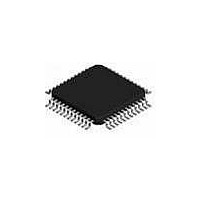
ispPAC-CLK5304S-01TN48I Lattice, ispPAC-CLK5304S-01TN48I Datasheet - Page 42

ispPAC-CLK5304S-01TN48I
Manufacturer Part Number
ispPAC-CLK5304S-01TN48I
Description
Clock Drivers & Distribution ISP 0 Delay Unv Fan- Out Buf-Sngl End I
Manufacturer
Lattice
Type
Zero Delay Programmable PLL Clock Generatorr
Datasheet
1.ISPPAC-CLK5308S-01TN48C.pdf
(56 pages)
Specifications of ispPAC-CLK5304S-01TN48I
Max Input Freq
267 MHz
Minimum Operating Temperature
- 40 C
Mounting Style
SMD/SMT
Supply Voltage (max)
3.6 V
Supply Voltage (min)
3 V
Maximum Operating Temperature
+ 85 C
Package / Case
TQFP-48
Lead Free Status / RoHS Status
Lead free / RoHS Compliant
Available stocks
Company
Part Number
Manufacturer
Quantity
Price
Company:
Part Number:
ISPPAC-CLK5304S-01TN48I
Manufacturer:
Lattice Semiconductor Corporation
Quantity:
10 000
Pin Descriptions – ispClock5304S, 5308S, 5312S
Lattice Semiconductor
VCCO_0
VCCO_1
VCCO_2
VCCO_3
VCCO_4
VCCO_5
GNDO_0
GNDO_1
GNDO_2
GNDO_3
GNDO_4
GNDO_5
BANK_0A
BANK_0B
BANK_1A
BANK_1B
BANK_2A
BANK_2B
BANK_3A
BANK_3B
BANK_4A
BANK_4B
BANK_5A
BANK_5B
VCCA
GNDA
VCCD
GNDD
REFA_REFP Clock Reference A/Positive Differential
REFB_REFN Clock Reference B/Negative Differential
REFSEL
VTT_REFA
FBK
VTT_FBK
VTT_REFB
VCCJ
TDO
TDI
TCK
TMS
Pin Name
Output Driver ‘0’ VCC
Output Driver ‘1’ VCC
Output Driver ‘2’ VCC
Output Driver ‘3’ VCC
Output Driver ‘4’ VCC
Output Driver ‘5’ VCC
Output Driver ‘0’ Ground
Output Driver ‘1’ Ground
Output Driver ‘2’ Ground
Output Driver ‘3’ Ground
Output Driver ‘4’ Ground
Output Driver ‘5’ Ground
Clock Output driver 0, ‘A’ output
Clock Output driver 0, ‘B’ output
Clock Output driver 1, ‘A’ output
Clock Output driver 1, ‘B’ output
Clock Output driver 2, ‘A’ output
Clock Output driver 2, ‘B’ output
Clock Output driver 3, ‘A’ output
Clock Output driver 3, ‘B’ output
Clock Output driver 4, ‘A’ output
Clock Output driver 4, ‘B’ output
Clock Output driver 5, ‘A’ output
Clock Output driver 5, ‘B’ output
Analog VCC for PLL circuitry
Analog Ground for PLL circuitry
Digital Core VCC
Digital GND
input
input
Clock Reference Select input (LVCMOS)
Termination voltage for reference input A
Feedback Input
Termination voltage for feedback input
Termination input for reference input B
JTAG interface VCC
JTAG TDO Output line
JTAG TDI Input line
JTAG Clock Input
JTAG Mode Select
3
3
3
Description
42
Pin Type
Output
Output
Output
Output
Output
Output
Output
Output
Output
Output
Output
Output
Output
Power
Power
Power
Power
Power
Power
Power
Power
Power
Power
Power
Power
Input
Input
Input
GND
GND
GND
GND
GND
GND
GND
GND
Input
Input
Input
Input
1
2
2
ispClock5304S
23, 24, 48
48 TQFP
ispClock5300S Family Data Sheet
21, 22
32
30
31
29
46
47
14
15
19
13
17
18
16
41
37
40
39
38
—
—
—
—
—
—
—
—
—
—
—
—
—
—
—
—
5
7
6
8
ispClock5308S
Pin Number
23, 24, 48
48 TQFP
21, 22
28
32
11
26
30
10
12
27
25
31
29
46
47
14
15
19
13
17
18
16
41
37
40
39
38
—
—
—
—
—
—
—
—
5
9
7
6
8
ispClock5312S
23, 24, 48
48 TQFP
21, 22
28
32
36
11
26
30
34
10
12
27
25
31
29
35
33
46
47
14
15
19
13
17
18
16
41
37
40
39
38
1
5
9
3
7
2
4
6
8


