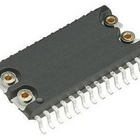
M48T86MH1 STMicroelectronics, M48T86MH1 Datasheet - Page 14

M48T86MH1
Manufacturer Part Number
M48T86MH1
Description
Real Time Clock USE 511-M48T86MH1E
Manufacturer
STMicroelectronics
Datasheet
1.M48T86MH1.pdf
(36 pages)
Specifications of M48T86MH1
Function
Clock, Calendar, Interrupt, Alarm
Rtc Memory Size
128 B
Supply Voltage (max)
5.5 V
Supply Voltage (min)
4.5 V
Maximum Operating Temperature
+ 70 C
Minimum Operating Temperature
0 C
Mounting Style
SMD/SMT
Rtc Bus Interface
Multiplexed
Package / Case
SO-28
Time Format
HH:MM:SS, Binary
Date Format
DW:DM:M:Y, Binary
Lead Free Status / RoHS Status
Lead free / RoHS Compliant
Available stocks
Company
Part Number
Manufacturer
Quantity
Price
Company:
Part Number:
M48T86MH1
Manufacturer:
CARTYS
Quantity:
2 585
Part Number:
M48T86MH1
Manufacturer:
ST
Quantity:
20 000
Clock operations
3
3.1
3.2
14/36
Clock operations
Address map
The address map of the M48T86 is shown in
10 bytes of RAM that contain the RTC time, calendar and alarm data, and 4 bytes which are
used for control and status. All bytes can be read or written to except for the following:
1.
2.
The contents of the four Registers A, B, C, and D are described in the “Registers” section.
Time, calendar, and alarm locations
The time and calendar information is obtained by reading the appropriate memory bytes.
The time, calendar, and alarm registers are set or initialized by writing the appropriate RAM
bytes. the contents of the time, calendar, and alarm bytes can be either binary or binary-
coded decimal (BCD) format. Before writing the internal time, calendar, and alarm register,
the SET bit (Register B; Bit 7) should be written to a logic '1.' This will prevent updates from
occurring while access is being attempted. In addition to writing the time, calendar, and
alarm registers in a selected format (binary or BCD), the data mode (DM) bit (Register B; Bit
2), must be set to the appropriate logic level ('1' signifies binary data; '0' signifies binary
coded decimal (BCD data). All time, calendar, and alarm bytes must use the same data
mode. The SET bit should be cleared after the data mode bit has been written to allow the
real-time clock to update the time and calendar bytes. Once initialized, the real-time clock
makes all updates in the selected mode. The data mode cannot be changed without
reinitializing the ten data bytes.
the time, calendar, and alarm locations. The 24/12 bit (Register B; Bit 1) cannot be changed
without reinitializing the hour locations. When the 12-hour format is selected, a logic '1' in
the high order bit of the hours byte represents PM. The time, calendar, and alarm bytes are
always accessible because they are double-buffered. Once per second the ten bytes are
advanced by one second and checked for an alarm condition. If a READ of the time and
calendar data occurs during an update, a problem exists where data such as seconds,
minutes, or hours may not correlate. However, the probability of reading incorrect time and
calendar data is low. Methods of avoiding possible incorrect time and calendar READs are
reviewed later in this text.
Registers C & D are “Read only.”
Bit 7 of Register A is “Read only.”
Table 3 on page 15
Figure
shows the binary and BCD formats of
8. It consists of 114 bytes of user RAM,
M48T86


