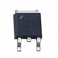
FDD8453LZ Fairchild Semiconductor, FDD8453LZ Datasheet
首页 Discrete Semiconductor Products MOSFETs, GaNFETs - Single FDD8453LZ
Manufacturer Part Number
FDD8453LZ
Description
MOSFET N-CH 40V 16.4A DPAK
Manufacturer
Fairchild Semiconductor
Specifications of FDD8453LZ
Fet Type
MOSFET N-Channel, Metal Oxide
Fet Feature
Logic Level Gate
Rds On (max) @ Id, Vgs
6.7 mOhm @ 15A, 10V
Drain To Source Voltage (vdss)
40V
Current - Continuous Drain (id) @ 25° C
16.4A
Vgs(th) (max) @ Id
3V @ 250µA
Gate Charge (qg) @ Vgs
64nC @ 10V
Input Capacitance (ciss) @ Vds
3515pF @ 20V
Power - Max
3.1W
Mounting Type
Surface Mount
Package / Case
DPak, TO-252 (2 leads+tab), SC-63
Configuration
Single
Transistor Polarity
N-Channel
Resistance Drain-source Rds (on)
0.0067 Ohm @ 10 V
Drain-source Breakdown Voltage
40 V
Gate-source Breakdown Voltage
+/- 20 V
Continuous Drain Current
16.4 A
Power Dissipation
3100 mW
Maximum Operating Temperature
+ 150 C
Mounting Style
SMD/SMT
Minimum Operating Temperature
- 55 C
Lead Free Status / RoHS Status
Lead free / RoHS Compliant
Available stocks
©2007 Fairchild Semiconductor Corporation
FDD8453LZ Rev.C
FDD8453LZ
N-Channel PowerTrench
40V, 50A, 6.7mΩ
Features
MOSFET Maximum Ratings
Thermal Characteristics
Package Marking and Ordering Information
V
V
I
E
P
T
R
R
D
DS
GS
AS
D
J
θJC
θJA
Max r
Max r
HBM ESD protection level >7kV typical (Note 4)
RoHS Compliant
, T
Symbol
Device Marking
STG
FDD8453LZ
DS(on)
DS(on)
= 6.7mΩ at V
= 8.7mΩ at V
Drain to Source Voltage
Gate to Source Voltage
Drain Current -Continuous (Package limited)
Single Pulse Avalanche Energy
Power Dissipation
Power Dissipation
Operating and Storage Junction Temperature Range
Thermal Resistance, Junction to Case
Thermal Resistance, Junction to Ambient
G
S
GS
GS
= 10V, I
= 4.5V, I
FDD8453LZ
(TO -252)
-Continuous
-Continuous (Silicon limited)
-Pulsed
D -PA K
Device
TO -2 52
D
D
= 15A
= 13A
T
®
C
D
= 25°C unless otherwise noted
MOSFET
Parameter
D-PAK (TO-252)
Package
1
T
T
T
T
T
General Description
This N-Channel MOSFET is produced using Fairchild
Semiconductor’s advanced PowerTrench
been especially tailored to minimize the on-state resistance and
switching loss. G-S zener has been added to enhance ESD
voltage level.
Applications
A
C
C
C
A
= 25°C
= 25°C
= 25°C
= 25°C
= 25°C
Inverter
Synchronous Rectifier
G
Reel Size
13’’
(Note 1a)
(Note 1a)
(Note 1a)
(Note 3)
D
S
Tape Width
12mm
-55 to +150
Ratings
16.4
±20
100
253
1.9
3.1
40
50
75
65
40
®
September 2007
process that has
www.fairchildsemi.com
2500 units
Quantity
Units
°C/W
mJ
°C
W
V
V
A
tm
Related parts for FDD8453LZ
FDD8453LZ Summary of contents
... R Thermal Resistance, Junction to Ambient θJA Package Marking and Ordering Information Device Marking Device FDD8453LZ FDD8453LZ ©2007 Fairchild Semiconductor Corporation FDD8453LZ Rev.C ® MOSFET General Description = 15A This N-Channel MOSFET is produced using Fairchild D Semiconductor’s advanced PowerTrench = 13A D been especially tailored to minimize the on-state resistance and switching loss ...
... Pulse Test: Pulse Width < 300µs, Duty cycle < 2.0%. ° 3: Starting 3mH 13A The diode connected between the gate and source serves only as protection against ESD. No gate overvoltage rating is implied. ©2007 Fairchild Semiconductor Corporation FDD8453LZ Rev 25°C unless otherwise noted J Test Conditions I = 250µ 250µA, referenced to 25°C ...
... PULSE DURATION = 80 s DUTY CYCLE = 0.5%MAX 150 GATE TO SOURCE VOLTAGE (V) GS Figure 5. Transfer Characteristics ©2007 Fairchild Semiconductor Corporation FDD8453LZ Rev 25°C unless otherwise noted J 4.0 µ s 3.5 3.0 2 3.5V GS 2.0 1.5 1 0.5 1.2 1.6 2 100 125 150 100 0.1 0.01 ...
... TIME IN AVALANCHE (ms) AV Figure 9. Unclamped Inductive Switching Capability Limited by Package 1.9 C/W θ CASE TEMPERATURE ( , T C Figure 11. Maximum Continuous Drain Current vs Ambient Temperature ©2007 Fairchild Semiconductor Corporation FDD8453LZ Rev 25°C unless otherwise noted J 4000 = 15V 1000 = 25V 100 1000 Figure 10. 200 100 V = 10V ...
... R = 1.9 θ JC 0.005 - DUTY CYCLE-DESCENDING ORDER 0.5 0.2 0.1 0.05 0.1 0.02 0.01 0.01 0.005 - ©2007 Fairchild Semiconductor Corporation FDD8453LZ Rev 25°C unless otherwise noted PULSE WIDTH (s) C RECTANGULAR PULSE DURATION (s) Figure 14. Transient Thermal Response Curve SINGLE PULSE C/W θ Note 1a ...
... Typical Characteristics 2 DUTY CYCLE-DESCENDING ORDER 0.5 0.2 0.1 0.1 0.05 0.02 0.01 0.01 0.002 - ©2007 Fairchild Semiconductor Corporation FDD8453LZ Rev 25°C unless otherwise noted J SINGLE PULSE C/W θ Note RECTANGULAR PULSE DURATION (s) Figure 16. Transient Thermal Response Curve NOTES: DUTY FACTOR PEAK T ...
... Product Status Advance Information Formative or In Design Preliminary First Production No Identification Needed Full Production Obsolete Not In Production ©2007 Fairchild Semiconductor Corporation FDD8453LZ Rev.C ® Green FPS™ Power247 Green FPS™ e-Series™ POWEREDGE GTO™ Power-SPM™ i-Lo™ PowerTrench IntelliMAX™ ...
Related keywords
fdd8444 fdd8447l fdd8447 fdd8445 fdd8444l fdd8453lz fdd8451 FDD8453LZ datasheet FDD8453LZ data sheet FDD8453LZ pdf datasheet FDD8453LZ component FDD8453LZ part FDD8453LZ distributor FDD8453LZ RoHS FDD8453LZ datasheet download


