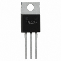
BUK9510-55A,127 NXP Semiconductors, BUK9510-55A,127 Datasheet - Page 2

BUK9510-55A,127
Manufacturer Part Number
BUK9510-55A,127
Description
MOSFET N-CH 55V 75A SOT78
Manufacturer
NXP Semiconductors
Series
TrenchMOS™r
Datasheet
1.BUK9510-55A127.pdf
(14 pages)
Specifications of BUK9510-55A,127
Fet Type
MOSFET N-Channel, Metal Oxide
Fet Feature
Logic Level Gate
Rds On (max) @ Id, Vgs
9 mOhm @ 25A, 10V
Drain To Source Voltage (vdss)
55V
Current - Continuous Drain (id) @ 25° C
75A
Vgs(th) (max) @ Id
2V @ 1mA
Gate Charge (qg) @ Vgs
68nC @ 5V
Input Capacitance (ciss) @ Vds
4307pF @ 25V
Power - Max
200W
Mounting Type
Through Hole
Package / Case
TO-220AB-3
Configuration
Single
Transistor Polarity
N-Channel
Resistance Drain-source Rds (on)
0.009 Ohms
Drain-source Breakdown Voltage
55 V
Gate-source Breakdown Voltage
+/- 15 V
Continuous Drain Current
75 A
Power Dissipation
200 W
Maximum Operating Temperature
+ 175 C
Mounting Style
Through Hole
Fall Time
139 ns
Minimum Operating Temperature
- 55 C
Rise Time
155 ns
Lead Free Status / RoHS Status
Lead free / RoHS Compliant
Other names
934056851127
BUK9510-55A
BUK9510-55A
BUK9510-55A
BUK9510-55A
Philips Semiconductors
5. Quick reference data
Table 2:
6. Limiting values
Table 3:
In accordance with the Absolute Maximum Rating System (IEC 60134).
[1]
[2]
9397 750 08555
Product data
Symbol Parameter
V
I
P
T
R
Symbol Parameter
V
V
V
I
I
P
T
T
Source-drain diode
I
I
Avalanche ruggedness
W
D
D
DM
DR
DRM
DS
tot
j
DS
DGR
GS
tot
stg
j
DSon
DSS
Current is limited by power dissipation chip rating
Continuous current is limited by package
drain-source voltage (DC)
drain current (DC)
total power dissipation
junction temperature
drain-source on-state resistance
drain-source voltage (DC)
drain-gate voltage (DC)
gate-source voltage (DC)
drain current (DC)
peak drain current
total power dissipation
storage temperature
operating junction temperature
reverse drain current (DC)
pulsed reverse drain current
non-repetitive avalanche energy
Quick reference data
Limiting values
Rev. 01 — 20 August 2001
Conditions
T
T
T
T
T
Conditions
T
Figure 2
T
T
Figure 3
T
T
T
unclamped inductive load; I
V
starting T
R
mb
mb
j
j
j
mb
mb
mb
mb
mb
mb
DS
GS
= 25 C; V
= 25 C; V
= 25 C; V
= 25 C; V
= 25 C
= 25 C; V
= 100 C; V
= 25 C; pulsed; t
= 25 C;
= 25 C
= 25 C; pulsed; t
BUK9510-55A; BUK9610-55A
= 20 k
55 V; V
and
mb
= 25 C
GS
GS
GS
3
Figure 1
GS
GS
GS
= 5 V; I
= 4.5 V; I
= 10 V; I
GS
= 5 V; R
= 5 V
= 5 V
= 5 V;
p
p
D
D
= 25 A
D
GS
10 s
10 s
Figure 2
= 25 A
= 25 A
D
= 50 ;
= 75 A;
TrenchMOS™ logic level FET
© Koninklijke Philips Electronics N.V. 2001. All rights reserved.
[1]
[1]
[2]
[2]
[1]
[2]
Typ
-
-
-
-
8
-
7
Min
-
-
-
-
-
-
-
-
-
-
-
-
55
55
Max
55
100
200
175
10
11
9
Max
55
55
100
75
70
400
200
+175
+175
100
75
400
333
15
Unit
V
A
W
m
m
m
Unit
V
V
V
A
A
A
A
W
A
A
A
mJ
C
C
C
2 of 14


